Wafer Chucks Electrostatic Chucks (ESC) Manufacturer
Description
Contact us: [email protected]
WhatsApp: +8613355741031
High-Performance Wafer Chucks | Vacuum & Electrostatic Chucks (ESC) Manufacturer
The Critical Foundation for Wafer Processing & Metrology
In the high-stakes world of semiconductor manufacturing, even microns matter. As a specialized wafer chuck manufacturer, we engineer precision vacuum chucks, advanced electrostatic chucks (ESC), and durable metal chucks to support the most demanding processes—from ultra-thin wafer handling to high-temperature etching and high-force applications.
Whether you are running a high-volume fab or a university research lab, our chucks provide the flatness, cleanliness, and durability required for zero-defect manufacturing.
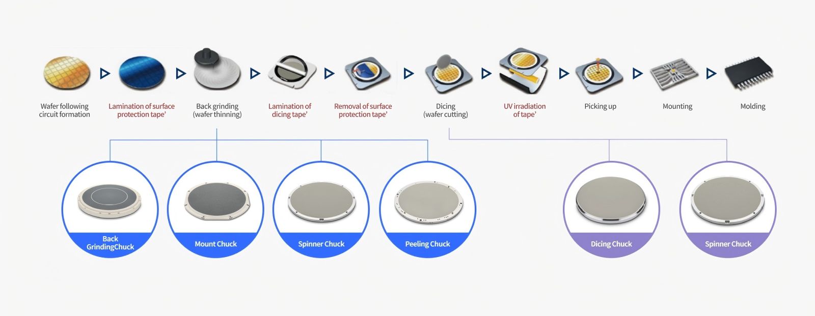
Product Series 1: Vacuum Wafer Chucks
Ideal for Probing, Dicing, and Thin Wafer Handling.
Our Vacuum Wafer Chucks utilize porous ceramic or multi-zone groove technology to provide a secure, warp-free grip on the backside of the wafer. Unlike standard chucks, our design minimizes bullseye marks and edge exclusion issues.
Material Options: High-purity Alumina (Al2O3), Silicon Carbide (SiC), or Porous Ceramic
Flatness: Superior parallelism down to < 5µm
Custom Sizes: From 2" (50mm) to 12" (300mm) and irregular dies (singulation)
Applications: Probe stations, wafer grinders, laser dicing, and pick-and-place systems
Special Feature: Multi-zone vacuum control to support ultra-thin (flexible) wafers without cracking
Product Series 2: Electrostatic Chucks (ESC)
Plasma & High-Temperature Stability.
For processes where physical contact via vacuum holes is not an option, our Electrostatic Chucks (ESC) are the solution. Using Coulombic or Johnsen-Rahbek (JR) principles, we provide a uniform clamping force across the entire wafer surface.
Technology: Coulombic Type (Alumina) & JR Type (Aluminum Nitride - AlN)
Thermal Control: Embedded heater pedestals and cooling channels for precise temperature management (-20°C to +200°C+)
Durability: Plasma-sprayed ceramic coatings to resist erosion in Etch and CVD environments
Customization: Single or bi-polar electrodes, embossed/grooved surfaces to purge backside gas (Helium) for thermal conduction
Refurbishment: We offer ESC refurbishment services to restore clamping force and extend lifespan at 40% cost of new
Product Series 3: Metal Wafer Chucks
Ideal for High-Force Probing, Thermal Cycling, and Cost-Effective Production.
Our Metal Wafer Chucks are precision-machined from stainless steel, aluminum alloy, or tool steel for applications requiring high mechanical strength, fast thermal response, or budget-friendly solutions. These chucks are widely used in R&D, manual probe stations, and high-throughput industrial environments where ceramic chucks are not mandatory.
Material Options: Stainless Steel (304, 316), Aluminum Alloy (6061, 7075), Tool Steel
Flatness: < 10µm to < 25µm depending on material and size
Custom Sizes: From 1" (25mm) to 12" (300mm) and custom shapes for MEMS or optoelectronics
Surface Finish: Precision ground, mirror polished, or with vacuum groove patterns
Vacuum Grooves: Concentric rings, spiral patterns, or custom multi-zone designs
Applications: Manual probe stations, high-force wafer probing, thermal chuck systems (-40°C to +150°C), pick-and-place equipment, and optical inspection
Key Advantages:
-
Excellent thermal conductivity for fast heating and cooling
-
High mechanical strength for heavy-duty probing without deformation
-
Lower cost compared to ceramic chucks
-
Easy to machine for rapid prototyping and custom geometries
-
Optional hard coating (Ni or DLC) for wear resistance and corrosion protection
Technical Specifications
| Specification | Vacuum Chuck (Ceramic) | Electrostatic Chuck (ESC) | Metal Vacuum Chuck |
|---|---|---|---|
| Wafer Size | 50mm – 300mm (Custom) | 150mm – 300mm | 25mm – 300mm (Custom) |
| Material | Alumina (96%/99.6%), SiC | Alumina (Coulomb), AlN (JR) | Stainless Steel, Aluminum Alloy, Tool Steel |
| Flatness | < 5µm (Global) | < 10µm | < 10µm to < 25µm |
| Operating Temp | -40°C to 150°C | -20°C to 400°C+ | -40°C to +150°C |
| Surface | Mirror polish / Porous | Embossed / Grooved / Dry etching | Precision ground / Mirror polish / Grooved |
| Lead Time | 2-4 Weeks | 4-6 Weeks | 1-3 Weeks |
Why Choose Us
Don't settle for off-the-shelf solutions. We are a direct manufacturer, not a middleman. This means lower costs, faster prototyping, and full customization.
In-House Ceramic & Metal Machining – We grind, polish, and mill both hard ceramics and precision metals in-house, ensuring absolute control over surface roughness, flatness, and profile.
Cleanroom Assembly – Assembled in Class 1000 (ISO 6) cleanrooms to prevent particle contamination.
100% Tested – Every chuck is tested for clamping force, leak rate, dielectric strength (for ESC), and high voltage breakdown (for ESC).
Local Support & Speed – As your local manufacturer, we offer 24-hour quotes and rapid turnaround for custom R&D chucks, including metal prototypes.
Applications
Our wafer chucks are mission-critical in the following sectors:
-
Semiconductor Front-End – Plasma Etching, CVD/PVD deposition, Lithography (Stepper)
-
Back-End & Assembly – Wafer probing (ATE), dicing, grinding, and backside metallization
-
Advanced Packaging – TSV (Through Silicon Via) and wafer bonding
-
R&D & Metrology – Probe stations, optical inspection systems, and digital holography (DHM)
-
High-Force & Thermal Testing – Metal chucks for thermal cycling and heavy-duty probing
Ready to upgrade your wafer handling?
Let us know your requirements. Whether you need a 300mm Electrostatic Chuck for an AMAT / TEL tool, a custom Vacuum Chuck for a non-standard substrate, or a rapid-turnaround Metal Chuck for your probe station, we have the solution.
We are committed to being your long-term partner in the semiconductor supply chain. Let's discuss your OEM specs today.
.jpg)
GET QUOTE
- Visit our website: https://www.nbyichou.com/
- Email us: [email protected]
- Call us/whatsapp: +86 13355741031
- Chat with us: Live chat support available on our website
People who viewed this item also viewed