Meta Description: Discover everything about Electrostatic Chucks (ESC) — principles, manufacturing, types (monopolar vs. bipolar), temperature control, and why they’re essential in semiconductor wafer processing. Learn the differences between ESC and vacuum chucks. Partner with YICHOU for custom ESC solutions.
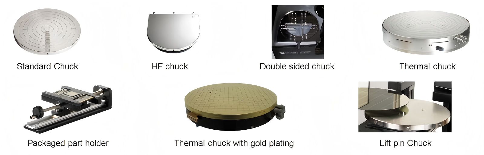
.png)
Introduction to Electrostatic Chucks (ESC): The Heart of Precision Manufacturing
In the high-stakes world of advanced manufacturing, particularly within the semiconductor industry, the ability to hold a workpiece with impeccable stability and precision is not just an advantage—it's an absolute necessity. At the forefront of this critical function is a sophisticated device known as an Electrostatic Chuck (ESC). Far more than a simple clamp, an ESC is a pinnacle of engineering that uses the fundamental force of electrostatics to secure objects, most commonly ultra-delicate silicon wafers, without any physical contact or mechanical stress.
YICHOU, a leading innovator in precision holding technology, stands at the vanguard of ESC design and manufacturing. As semiconductor features shrink to nanometer scales and process tolerances become ever more stringent, the role of the ESC has evolved from a supportive component to a cornerstone of process yield and reliability. This guide will delve into the principles, types, applications, and critical advantages of electrostatic chucks, explaining why they have become the undisputed standard in environments where vibration, contamination, and thermal distortion are the enemies of progress.
How Does an Electrostatic Chuck Work? The Principle of Invisible Force
The operation of an electrostatic chuck is a brilliant application of one of nature's fundamental forces. To understand it, we must start with electrostatics—the study of stationary electric charges. The core principle is Coulomb's Law, which states that opposite electric charges attract each other, while like charges repel. An ESC masterfully harnesses this attraction.
An ESC typically consists of a dielectric layer (often made from high-performance ceramics like aluminum nitride or alumina) on top of one or more conductive electrodes. Here is a step-by-step breakdown of the process:
-
Placement: A wafer or workpiece is placed on the smooth surface of the ESC.
-
Charging: A high-voltage DC power supply (ranging from hundreds to thousands of volts) is applied to the embedded electrode(s). This creates a strong electrostatic field.
-
Polarization: While the wafer itself is typically a semiconductor (like silicon) and not a perfect conductor, the powerful electric field induces a polarization of charges within it. Positive charges in the wafer align toward the negative electrode, and negative charges align toward the positive electrode.
-
Attraction: This induced charge separation creates a powerful electrostatic attraction force between the wafer and the electrodes of the ESC, clamping the wafer firmly and uniformly to the surface.
This method of holding is non-mechanical. There are no pins, clamps, or suction holes that could cause stress, shadowing, or particle generation. The holding force is distributed evenly across the entire backside of the wafer, ensuring exceptional flatness (planarity) and uniform thermal contact—both critical for processes like lithography and etching.
Monopolar vs. Bipolar Electrostatic Chucks: Choosing the Right Tool
Not all electrostatic chucks are created equal. The design of the electrode system categorizes ESCs into two primary types, each suited for specific applications.
Monopolar (or Johnsen-Rahbek) ESC
-
Principle: Uses a single-pole electrode and relies on a slight, controlled electrical conductivity in the dielectric layer. The holding force is generated at the microscopic level due to the very close proximity of charges (the Johnsen-Rahbek effect), resulting in an extremely strong clamping force.
-
Advantages: Very high clamping force, allowing for secure holding of thicker or warped wafers. Generally operates at lower voltages.
-
Disadvantages: Requires a slightly conductive dielectric, which can lead to minor leakage currents. This can be a concern for some ultra-sensitive processes. Thermal management can be more complex.
-
Best For: Processes where maximum mechanical stability is paramount, and minimal electrical interference is acceptable.
Bipolar (or Coulombic) ESC
-
Principle: Uses two (or more) interdigitated electrodes of opposite polarity embedded within a perfect insulator. The holding force is purely based on Coulombic attraction with the induced charges in the wafer.
-
Advantages: No DC current flows through the wafer, eliminating the risk of electrical damage or interference to sensitive devices on the wafer (a critical factor in semiconductor fabrication). Typically offers superior and more responsive temperature control.
-
Disadvantages: Generally provides a lower clamping force per applied voltage compared to the monopolar type.
-
Best For: The vast majority of modern semiconductor processes—especially plasma-based processes like etching and chemical vapor deposition (CVD), where electrical isolation is critical.
YICHOU engineers excel at designing and manufacturing both monopolar and bipolar ESCs, providing tailored solutions based on the specific process requirements, whether for R&D, advanced packaging, or leading-edge wafer fabrication.
The Art and Science of ESC Manufacturing
Creating a reliable, high-performance electrostatic chuck is a feat of advanced materials science and precision engineering. The manufacturing process is multi-stage and demands extreme cleanliness and accuracy.
-
Material Selection: The base material is crucial. High-purity, fine-grain aluminum nitride (AlN) is a top choice due to its excellent thermal conductivity, good dielectric strength, and thermal expansion coefficient close to silicon. Alumina (Al₂O₃) is another common, cost-effective option.
-
Electrode Fabrication: The electrode pattern (single for monopolar, interdigitated for bipolar) is created using techniques akin to semiconductor manufacturing, such as thin-film deposition (sputtering) and photolithography. YICHOU utilizes state-of-the-art patterning to ensure electrode uniformity, which is key to consistent clamping and heating.
-
Dielectric Layer Application: A thick, flawless dielectric layer is applied over the electrodes. This is often done via plasma spraying or screen-printing followed by high-temperature sintering. The thickness, density, and purity of this layer directly impact the chuck's voltage rating, reliability, and thermal performance.
-
Surface Finishing: The wafer-contact surface is polished to a mirror finish (often Ra < 0.4 µm) to maximize the contact area for both clamping and heat transfer. Any micro-roughness can trap particles or create air gaps that degrade thermal uniformity.
-
Integration & Testing: The ceramic body is bonded to a cooling baseplate (often with embedded channels for helium backside cooling). Electrical feedthroughs are installed. Each chuck undergoes rigorous testing for insulation resistance, breakdown voltage, clamping force uniformity, and—critically—temperature control performance.
The Critical Role of Temperature Control in ESCs
In semiconductor processing, thermal management is not an afterthought; it is a process parameter. Processes like plasma etching generate significant heat on the wafer surface, which can distort patterns and reduce yield if not controlled.
This is where the Electrostatic Chuck with Integrated Temperature Control becomes a system, not just a clamp. YICHOU's advanced ESCs integrate sophisticated thermal management:
-
Helium Backside Cooling: The polished ESC surface is never perfectly flat at the atomic level. A small gap exists between the wafer and chuck. Helium gas, injected into this gap, fills the micro-voids, creating an excellent conductive path for heat transfer from the wafer to the chuck.
-
Embedded Heaters & Sensors: Multi-zone resistive heaters and RTD (Resistance Temperature Detector) sensors are embedded within the ESC structure. A closed-loop control system constantly reads the temperature and adjusts heater power to maintain the wafer at a setpoint with astonishing uniformity (often within ±0.5°C across a 300mm wafer).
-
Chilled Baseplate: The back of the ESC is typically attached to a water-cooled baseplate, which acts as a heat sink to remove the energy conducted from the wafer.
This precise thermal regulation ensures process repeatability, critical dimension control, and prevents wafer warping.
.jpg)
ESC vs. Vacuum Chuck vs. Magnetic Chuck: A Comparative Analysis
To appreciate the ESC's value, it's helpful to compare it with alternative workholding technologies.
| Feature | Electrostatic Chuck (ESC) | Vacuum Chuck | Magnetic Chuck |
|---|---|---|---|
| Holding Principle | Electrostatic attraction | Atmospheric pressure differential | Magnetic attraction |
| Contact | Full-area, non-mechanical | Full-area, requires seal | Mechanical contact with poles |
| Particle Generation | Very Low (no moving parts) | Medium (seals can wear) | High (metal-on-metal contact) |
| Planarity/Flatness | Excellent (uniform force) | Good (depends on seal/flatness) | Poor (holds only at poles) |
| Thermal Contact | Excellent (with He cooling) | Poor (air is an insulator) | Poor |
| Applicable Materials | Semiconductors, insulators, conductors | Mostly non-porous materials | Only ferromagnetic materials |
| Vacuum Environment | Ideal (no pumps needed) | Impossible (relies on pressure) | Possible |
| Process Examples | Wafer etching, CVD, lithography | CNC machining of composites, glass | Surface grinding of steel parts |
The Verdict: For the semiconductor industry's cleanroom, vacuum, and plasma environments, the ESC is unrivaled. Vacuum chucks fail in low-pressure chambers, and magnetic chucks are useless for silicon wafers and generate unacceptable contamination. The ESC’s clean, reliable, and electrically controllable clamping is perfectly matched to fab needs.
Why ESCs are Indispensable in Semiconductor Wafer Processing
The semiconductor fabrication line is where the ESC proves its true worth. At every critical step, it enables the precision required to build billion-transistor chips:
-
Plasma Etching & Deposition (CVD/PVD): In these vacuum chambers, wafers are bombarded by reactive ions or coated with thin films. The ESC securely holds the wafer against plasma forces while precisely controlling its temperature to ensure etching or deposition uniformity. The electrical properties of a bipolar ESC also help control the plasma sheath at the wafer surface.
-
Lithography: During photolithography, the wafer must be held perfectly flat (within nanometers) under the stepper lens. An ESC provides the necessary ultra-planarity and stability to ensure pattern fidelity across the entire wafer.
-
Inspection & Metrology: Tools like scanning electron microscopes (SEMs) require the sample to be absolutely still. ESCs provide vibration-free clamping for high-resolution imaging and measurement.
Without ESCs, the advancement of Moore's Law and the production of modern microprocessors and memory chips would be impossible.
Why Choose YICHOU for Your Electrostatic Chuck Needs?
At YICHOU, we don’t just manufacture ESCs; we engineer custom holding solutions that maximize your process yield and uptime. Whether you need a monopolar ESC for high-force clamping, a bipolar ESC for plasma-sensitive applications, or a multi-zone temperature-controlled ESC for advanced lithography or etching, YICHOU delivers.
What sets YICHOU apart?
-
Fully Custom Designs: From 50mm to 450mm wafer sizes, odd-shaped substrates, and special dielectric materials — we build to your exact specifications.
-
Rapid Prototyping & Short Lead Times: Our in-house ceramic processing and thin-film deposition facilities allow us to deliver samples in weeks, not months.
-
Technical Support & Integration: Our application engineers work with your team to optimize clamping voltages, helium backside cooling parameters, and temperature control algorithms.
-
Proven Reliability: YICHOU ESCs are installed in leading semiconductor fabs, R&D centers, and equipment OEMs worldwide — with thousands of field-proven units.
Frequently Asked Questions (FAQs)
Q: Do ESCs control voltage or current?
A: ESCs are primarily voltage-controlled devices. A high-voltage DC power supply applies a specific voltage to the electrodes to generate the electrostatic field. The resulting current flow is typically minimal (microamps), especially in a well-designed bipolar ESC.
Q: What are the advantages of electrostatic motors?
A: While different from ESCs, electrostatic motors (using attraction/repulsion between charged plates) offer advantages in micro-electromechanical systems (MEMS): they are simple to fabricate with silicon processes, require very low power at small scales, and generate no magnetic fields.
Q: Are magnetic chucks safe to use?
A: Magnetic chucks are safe for their intended purpose—holding ferromagnetic workpieces in machining. Key safety points include: ensuring the workpiece fully covers the poles to maintain grip, keeping hands clear during activation/deactivation, and not using them near people with pacemakers due to strong magnetic fields.
Q: Can epoxy cure in a vacuum?
A: Yes, and it's often beneficial. Vacuum curing, often used with vacuum casting processes, removes air bubbles trapped in the epoxy, resulting in a void-free, stronger, and optically clear cast part. The vacuum lowers the boiling point of volatiles, allowing them to escape before curing.
Q: What is an electrostatic gun used for?
A: An electrostatic gun, commonly used in electrostatic powder coating and painting, applies a charge to particles (paint or powder). The charged particles are then attracted to the grounded workpiece, ensuring a uniform, wrap-around coating with high material transfer efficiency and less overspray.
Q: What is the alternative to vacuum casting?
A: A common alternative is pressure casting, where the material (like resin) is injected into a mold under positive pressure. This also helps minimize voids and can be faster for certain applications, though it requires different equipment.
Conclusion: The Future is Held by Electrostatic Forces
From securing the world's most advanced silicon wafers to enabling new technologies in displays and compound semiconductors, the electrostatic chuck is a testament to how mastering a fundamental physical principle can drive an entire industry forward. Its non-contact, clean, and controllable nature makes it irreplaceable in high-precision, high-value manufacturing.
As semiconductor devices continue to evolve—moving to 3D architectures, new materials like silicon carbide and gallium nitride, and larger wafer sizes—the demands on the ESC will only grow. YICHOU is committed to this future, continuously innovating in chuck materials, thermal management solutions, and control systems to meet the next generation of manufacturing challenges.
.jpg)
GET QUOTE
- Visit our website: https://www.nbyichou.com/
- Email us: [email protected]
- Call us/whatsapp: +86 13355741031
- Chat with us: Live chat support available on our website