Meta Description: Discover the critical role of the wafer vacuum chuck in semiconductor manufacturing. Learn how it works, its advantages over electrostatic chucks, and why it's essential for precision wafer fabrication.
Introduction: The Unseen Hero of Semiconductor Manufacturing
In the pristine, controlled chaos of a semiconductor fabrication plant (fab), where billions of transistors are etched onto a sliver of silicon thinner than a human hair, precision is not just a goal—it is an absolute necessity. The margin for error is zero. At the heart of this nanoscale ballet lies a critical but often overlooked component: the wafer vacuum chuck.
This sophisticated workholding device is the fundamental interface between the delicate silicon wafer and the multi-million dollar machinery that patterns, etches, and inspects it. It is the bedrock upon which modern electronics are built. A failure in this component means misalignment, defects, and catastrophic yield loss. Understanding the wafer vacuum chuck—its function, its advantages, and its role in the larger ecosystem of semiconductor manufacturing—is key to appreciating the engineering marvel that is the modern chip.
This comprehensive guide will demystify the vacuum wafer chuck. We will explore its operating principles, delve into its design, compare it with competing technologies like electrostatic chucks, and answer the most frequently asked questions sourced directly from engineers and technicians in the field.
What is a Wafer Vacuum Chuck? The Fundamental Interface
At its core, a wafer vacuum chuck is a precision workholding device designed specifically to secure thin, flat substrates—primarily silicon wafers—during various fabrication, metrology, and testing processes. It operates on a simple yet profoundly effective physical principle: the use of a pressure differential to generate a clamping force.
Imagine placing a flat object on a surface and then sucking all the air out from between them. The external atmospheric pressure, which is now significantly higher, pushes the object down onto the surface with considerable force. This is the essence of a vacuum chuck.
The surface of a wafer vacuum chuck is not perfectly smooth. It is machined to extreme flatness, often within microns, and features a precise pattern of microscopic grooves, pores, or seals. When a vacuum pump evacuates air from these channels, it creates a low-pressure zone. The atmospheric pressure acting on the top side of the wafer (approximately 14.7 PSI at sea level) then clamps it uniformly and securely against the chuck's surface, without any mechanical distortion or contamination.
How Does a Vacuum Wafer Chuck Work? A Step-by-Step Breakdown
The operation of a vacuum wafer chuck is a elegant sequence of engineered steps:
-
Placement & Initial Positioning: A robotic automation system, often a wafer handler, carefully picks a silicon wafer from a cassette (FOUP) and places it onto the prepared surface of the vacuum chuck. Precision alignment pins or vision systems ensure the wafer is correctly oriented.
-
Evacuation & Vacuum Generation: A command signal activates a vacuum pump. This pump rapidly removes air from the internal plenum and the network of grooves on the chuck's face. The system is connected via sealed ports and vacuum lines. A critical component here is the vacuum filter, which prevents any particulate matter from the pump or lines from contaminating the chuck or wafer.
-
Pressure Differential & Clamping Force Generation: As air is evacuated, the pressure in the grooves (P_internal) drops significantly below the external atmospheric pressure (P_atmospheric). According to the basic formula Force = Pressure × Area, the resulting clamping force (F_clamp) is calculated as:
F_clamp = (P_atmospheric - P_internal) × A
where A is the effective area sealed by the vacuum. For a standard 300mm wafer, this can generate a substantial holding force distributed perfectly evenly across the wafer's entire backside. -
Stable Processing: With the wafer held perfectly flat and immovable, the manufacturing process—whether it be photolithography, optical inspection, or laser dicing—can proceed with nanometric accuracy. The chuck often incorporates thermal control channels to manage the wafer's temperature during these steps.
-
Release & Transfer: Upon process completion, the vacuum is vented in a controlled manner by introducing clean, dry air or nitrogen back into the system. This equalizes the pressure above and below the wafer, instantly nullifying the clamping force. The robot can then safely lift the wafer and transfer it to the next stage.
Key Advantages of Using a Vacuum Chuck for Wafers
The prevalence of the vacuum wafer chuck is no accident. It offers a suite of compelling advantages that make it ideal for semiconductor applications:
-
Exceptional Flatness and Stability: Mechanical chucks can induce stress and cause wafer bowing. The vacuum chuck's uniform pressure distribution pulls the wafer into perfect conformity with its ultra-flat surface, eliminating distortion. This is non-negotiable in photolithography, where depth of focus is measured in nanometers.
-
Minimal Contamination Risk: The semiconductor world is a war on particles. Unlike adhesive tapes or mechanical clamps with moving parts, vacuum chucks are passive and contact only the wafer's non-active backside. This "clean" holding method drastically reduces the risk of generating contaminants or leaving residue.
-
Superior Thermal Management: The full-surface contact between the wafer and the chuck provides an excellent path for conductive heat transfer. This allows for efficient cooling during processes that generate heat (e.g., laser machining) or precise temperature control via embedded heaters or coolers in the chuck body.
-
Compatibility with Ultra-Thin and Fragile Wafers: As the industry moves towards thinner wafers for advanced packaging and 3D integration, mechanical handling becomes riskier. Vacuum chucks provide gentle, distributed clamping force that minimizes the risk of cracking or warping these delicate substrates.
-
Simplicity, Reliability, and Cost-Effectiveness: With no need for high-voltage electronics (like electrostatic chucks) or complex control systems, vacuum chucks are generally more reliable, easier to maintain, and less expensive to implement and operate.
.jpg)
Vacuum Chuck vs. Electrostatic Chuck: A Critical Semiconductor Showdown
One of the most common and important comparisons in semiconductor workholding is between the vacuum chuck and the electrostatic chuck (ESC). While both secure wafers, their underlying physics and ideal applications are vastly different. The choice between them is often the first critical decision in process tool design.
| Feature | Vacuum Wafer Chuck | Electrostatic Chuck (ESC) |
|---|---|---|
| Clamping Principle | Atmospheric pressure differential | Coulombic Chucking (for monopolar) or Johnsen-Rahbek forces (for bipolar). This involves applying a high voltage to create an electrostatic attraction. |
| Clamping Force | Good and consistent, directly proportional to vacuum level. | Can be very high and rapidly controlled, especially with bipolar electrostatic chuck designs. |
| Operating Environment | Requires an atmosphere (air/N2). Becomes ineffective in a vacuum. | Can operate perfectly in a vacuum environment. This is its killer application. |
| Heat Transfer | Good conductive cooling. | Excellent; often integrated with high-power electrostatic chuck He for active, precise temperature control from -50°C to over 200°C. |
| Contamination Risk | Very low; purely mechanical. | Low, but potential for micro-arcsing or attraction of charged particles. |
| Wafer Types | Universal for standard conductive and insulating wafers. | Performance can vary with wafer resistivity. Special designs are needed for highly resistive materials. |
| Complexity & Cost | Generally lower. A simpler system with a pump and valves. | Generally higher. Requires high-voltage DC power supplies and sophisticated control systems. |
When to Use Which: A Practical Guide
-
Use a Vacuum Wafer Chuck when:
-
The process occurs at atmospheric pressure (e.g., metrology, inspection, dicing, packaging).
-
Cost and simplicity are primary drivers.
-
The process does not require extreme, active wafer heating or cooling.
-
You are handling a variety of wafer materials without concern for their electrical properties.
-
-
Use an Electrostatic Chuck when:
-
The process occurs inside a vacuum chamber (e.g., plasma etching, Chemical Vapor Deposition (CVD), Physical Vapor Deposition (PVD)).
-
You require precise and powerful temperature control (electrostatic chuck He is standard).
-
You need very high clamping force for processes with significant mechanical stress.
-
The difference between monopsia and bipolar electrostatic chuck designs often comes down to the type of wafer and the required force. Bipolar ESCs are more common and provide higher clamping forces for a given voltage, making them suitable for a wider range of applications.
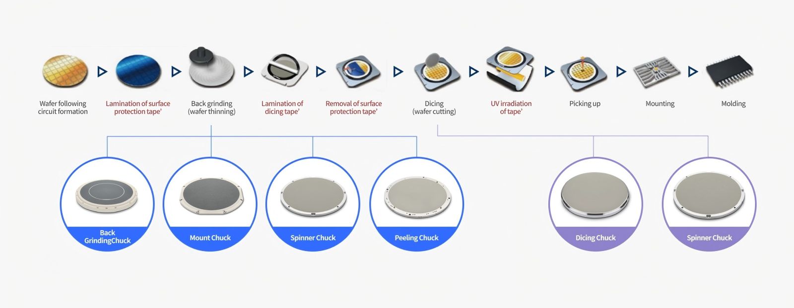
Common Applications of Wafer Vacuum Chucks in the Fab
The wafer vacuum chuck is a workhorse found throughout the semiconductor production line:
-
Photolithography: This is arguably its most critical application. Before a wafer is exposed to light through a photomask, it must be held perfectly flat on the lithography scanner's stage. Any deviation, or "non-coplanarity," results in blurry patterns and ruined chips. The vacuum chuck here is a masterpiece of thermal and mechanical stability.
-
Metrology and Inspection: Tools that measure critical dimensions, film thickness, or surface defects require a rock-steady platform. Vacuum chucks hold wafers motionless for high-resolution scanning electron microscopes (SEMs), atomic force microscopes (AFMs), and optical inspection systems.
-
Wafer Dicing and Scribing: When a completed wafer is cut into individual dies (chips), it is mounted on a dicing frame with tape. A vacuum chuck underneath secures the entire assembly during the high-speed sawing or laser ablation process, preventing vibration-induced chipping and ensuring clean, precise streets between dies.
-
Packaging and Testing: In the back-end of the line, vacuum chucks are used for processes like wafer-level packaging, bumping, and final test and burn-in, where stability and cleanliness remain paramount.
Why Choose YICHOU for Your Wafer Vacuum Chuck Needs?
【Custom Purchase Encouragement Section】
At YICHOU, we understand that no two wafer processes are identical. Whether you need a porous ceramic vacuum chuck for ultra‑thin wafer backgrinding, a grooved metal chuck for high‑throughput inspection, or a custom shape for odd‑sized substrates (e.g., GaAs, SiC, glass panels), YICHOU delivers precision, cleanliness, and reliability.
Why leading fabs and OEMs choose YICHOU:
-
Custom Engineering – We design chucks to your exact wafer diameter, flatness spec (≤ 5 µm TIR), vacuum hole pattern, and material (porous alumina, silicon carbide, stainless steel, or anodized aluminum).
-
Ultra‑Clean Manufacturing – All chucks are fabricated and packaged in Class 10 (ISO 4) cleanrooms, with ultrasonic cleaning and vacuum‑bag sealing to ensure particle‑free delivery.
-
Rapid Turnaround – Standard sizes (150 mm, 200 mm, 300 mm) available from stock. Custom prototypes delivered in as few as 10 business days.
-
Expert Support – Our application engineers help you select the right groove geometry, porosity level, and vacuum port configuration to maximize holding force while minimizing wafer bow or backside marking.
-
Proven in Production – YICHOU vacuum chucks are trusted by semiconductor equipment manufacturers, R&D labs, and OSAT facilities worldwide.
Special offer for first‑time customers:
Contact YICHOU today and mention this article to receive a free flatness measurement report with your first custom chuck order.
Frequently Asked Questions (FAQ)
Q: What are wafer chucks made of?
A: Wafer vacuum chucks are manufactured from high-grade, non-magnetic, and thermally stable materials. Common choices include:
-
Stainless Steel (e.g., 17-4PH): Offers excellent strength, corrosion resistance, and machinability.
-
Aluminum (e.g., 6061-T6): Lighter and easier to machine, often used where weight is a concern.
-
Ceramics (e.g., Alumina, AlN): Used in high-temperature applications or where extreme thermal conductivity (like Aluminum Nitride) is needed for temperature control.
Q: What is the purpose of a chuck in a general sense?
A: The fundamental purpose of a chuck, whether on a lathe or in a semiconductor tool, is to securely hold a workpiece in a precise location and orientation while a manufacturing operation is performed on it. It is the critical link between the tool and the part.
Q: Can you use a vacuum chuck in a vacuum chamber?
A: No, this is a fundamental limitation. A vacuum chuck relies on the presence of atmospheric pressure to create the clamping force. Inside a vacuum chamber, where the external pressure is also low, the pressure differential vanishes, and the clamping force ceases to exist. This is the primary reason electrostatic chucks were developed and dominate vacuum-based processes.
Q: How do vacuum filters work and why are they important?
A: Vacuum filters are essential components placed in the line between the vacuum pump and the chuck. They work by trapping particulate matter, moisture, and oil aerosols. In a wafer vacuum chuck system, they prevent contamination from the pump from traveling upstream and settling on the pristine chuck surface or the backside of the wafer, which could cause flatness issues or particle defects.
Q: What are the disadvantages of magnetic chucks, and why aren't they used for wafers?
A: Magnetic chucks are superb for holding ferrous materials in grinding or milling applications. Their main disadvantages make them completely unsuitable for semiconductor wafers:
-
They only work on magnetic materials. Silicon is non-magnetic.
-
They can induce residual magnetism in the workpiece.
-
They generate heat due to eddy currents.
-
They can attract ferrous particles, creating a massive contamination risk.
While magnetic chucks are robust for industrial metalworking, they have no place in a cleanroom environment.
Q: What is the main benefit of vacuum concrete? (And why does it appear in search results?)
A: This is a great example of how "Also Asked" algorithms work. The term "vacuum" is the connector. The main benefit of vacuum concrete is the rapid dewatering of freshly poured concrete slabs through a vacuum mat. This increases early strength, reduces permeability, and improves the surface finish. It's a completely different application of vacuum technology, in civil engineering rather than semiconductors, but it shares the core principle of using a pressure differential for a practical effect.
Conclusion: The Indispensable Foundation of Precision
The wafer vacuum chuck stands as a testament to the idea that the most impactful solutions are often elegantly simple. While it may lack the high-tech allure of an EUV lithography scanner or the complex physics of an electrostatic chuck, it remains an indispensable foundation of the entire semiconductor industry.
Its ability to provide clean, stable, and reliable clamping for the world's most valuable and delicate substrates enables the continued advancement of Moore's Law. As new challenges emerge—such as handling larger, thinner wafers for advanced packaging or managing thermal loads in next-generation power devices—the fundamental principle of the vacuum wafer chuck will continue to be adapted and refined.
At YICHOU, we specialize in designing and manufacturing high-performance vacuum chucks that meet these evolving demands. With a focus on precision, cleanliness, and reliability, our solutions support critical processes across semiconductor fabrication, advanced packaging, and beyond.
For engineers, procurement specialists, and industry partners seeking to optimize their chuck performance or develop custom clamping solutions:
Let’s discuss your requirements.
Contact YICHOU today for a tailored consultation or to request a quote.
.jpg)
GET QUOTE
- Visit our website: https://www.nbyichou.com/
- Email us: [email protected]
- Call us/whatsapp: +86 13355741031
- Chat with us: Live chat support available on our website