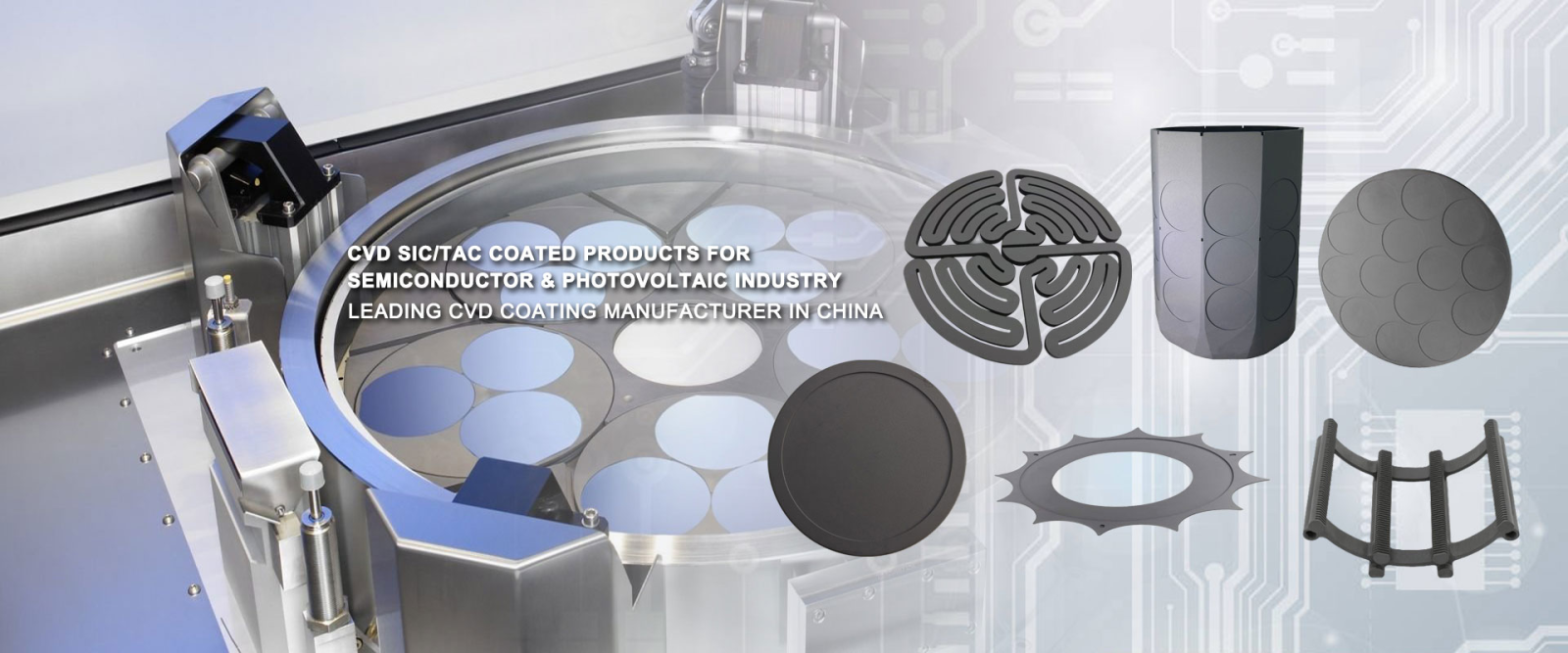
Introduction: The Unsung Hero of Semiconductor Fabrication
In the gleaming cleanrooms of semiconductor fabs, where billions of transistors are etched onto slices of silicon thinner than a human hair, precision isn't just a goal—it's an absolute necessity. While much attention is given to photolithography scanners, etching tools, and deposition systems, there exists a humble, often overlooked component that makes all this microscopic magic possible: the wafer chuck.
Imagine trying to write on a grain of rice with nanometer-scale accuracy while it's vibrating, warping, or shifting by even a thousandth of a millimeter. Impossible, right? That's exactly the challenge semiconductor manufacturers face—and it's the wafer chuck that solves it. This seemingly simple device holds the silicon wafer firmly in place during every critical processing step, from coating and exposure to inspection and testing.
As the semiconductor industry pushes further into the era of 3nm, 2nm, and beyond, the role of the wafer chuck has evolved from passive support to active precision engineering. In this comprehensive guide, we'll explore everything you need to know about wafer chucks, their critical function in chip manufacturing, and why companies like YICHOU are at the forefront of this essential technology.
What is a Wafer Chuck? – The Core Definition
A wafer chuck is a specialized holding device designed to secure silicon wafers during semiconductor fabrication processes with exceptional precision, stability, and flatness. Unlike conventional clamps or fixtures, wafer chucks must meet extraordinary requirements: they must hold wafers without causing damage, contamination, or distortion while maintaining positional accuracy at the nanometer scale.
The Basic Function:
-
Secure Positioning: Prevents any movement during high-speed spinning, scanning, or processing
-
Flatness Maintenance: Ensures the wafer remains perfectly flat across its entire surface
-
Thermal Management: Dissipates heat generated during processes or maintains specific temperatures
-
Electrical Connectivity: Provides ground paths or electrical bias when needed
-
Contamination Control: Minimizes particle generation and is compatible with cleanroom environments
Types of Wafer Chucks:
-
Electrostatic Chucks (ESCs): The most common type in advanced semiconductor fabs
-
Use electrostatic attraction between the chuck and wafer
-
No mechanical contact means minimal contamination
-
Excellent for vacuum environments
-
-
Vacuum Chucks:
-
Use suction through precisely placed holes
-
Simpler design but effective for many applications
-
Common in metrology and inspection equipment
-
-
Mechanical Chucks:
-
Use physical clamps or edge grips
-
Less common in front-end processing due to contamination risk
-
Still used in some packaging and testing applications
-
Why is it Called a "Chuck"? – Etymology & Naming
The term "chuck" might seem oddly informal for such precision equipment, but its origins reveal a logical progression. In traditional machining and woodworking, a chuck refers to a clamping device that holds a rotating tool or workpiece—most familiarly in lathes, drills, and milling machines.
The word itself dates back to the 17th century, possibly derived from "chock" (a wedge or block) or the Old French "choquer" (to strike or shock). In machining contexts, it first appeared as a device that "chucks" or grips workpieces securely.
When semiconductor manufacturing emerged in the mid-20th century, engineers adapted familiar terminology from precision machining. The wafer "chuck" performed a conceptually similar function to its mechanical predecessors: holding a workpiece (the wafer) securely during processing. However, the similarities largely end there—modern semiconductor wafer chucks operate at precision levels thousands of times greater than their mechanical namesakes.
This naming convention extends to related equipment like chuck tables, which are essentially specialized chucks used in wafer dicing (the process of cutting individual chips from the wafer). While both are "chucks," their designs and applications differ significantly.
The Critical Role of a Wafer Chuck in Chip Manufacturing
To appreciate why wafer chucks deserve more attention, consider these critical functions they perform in semiconductor fabrication:
1. Nanometer-Scale Precision Holding
Modern EUV (Extreme Ultraviolet) lithography systems pattern features as small as 13 nanometers—approximately 1/6000th the width of a human hair. At this scale, even thermal expansion from body heat or minuscule vibrations from floor movement can ruin an entire wafer. Premium wafer chucks from manufacturers like YICHOU maintain positional stability within single-digit nanometers.
2. Thermal Management Excellence
Many semiconductor processes generate significant heat:
-
Plasma etching can locally heat wafers to 100+°C
-
Ion implantation creates surface heating
-
Even exposure to intense laser light in inspection systems causes thermal expansion
Advanced wafer chucks incorporate sophisticated cooling systems, often using helium backside cooling, to maintain wafers at consistent temperatures (±0.1°C) across the entire surface. This thermal stability prevents pattern distortion and ensures uniform processing.
3. Flatness and Focus Maintenance
In photolithography, the entire wafer surface must remain within the extremely narrow focal plane of the scanner. Even microscopic bowing or warping—as little as 50 nanometers—can render parts of the wafer out of focus. Wafer chucks counter this by:
-
Applying corrective forces to flatten wafers
-
Using adaptive surfaces that conform to wafer topography
-
Maintaining vacuum or electrostatic force distribution that minimizes distortion
4. Yield Protection
A single particle contaminant measuring just 10 nanometers can kill a modern transistor. Wafer chucks designed with cleanroom compatibility in mind:
-
Use non-particle-generating materials
-
Incorporate surface treatments that minimize adhesion
-
Feature designs that eliminate particle-trapping crevices
-
Enable gentle wafer handling to prevent microfractures
YICHOU's wafer chucks, for instance, employ proprietary ceramic compounds that offer exceptional hardness, minimal thermal expansion, and virtually no particle generation even after millions of cycles.
5. Process Flexibility
Different semiconductor processes have different chuck requirements:
-
Lithography: Maximum flatness and thermal stability
-
Etching: Plasma resistance and electrical characteristics
-
Inspection: Rapid exchange capabilities and minimal interference
-
Metrology: Extreme precision and reproducibility
Leading manufacturers like YICHOU offer application-specific chuck designs optimized for each process step while maintaining compatibility with major equipment platforms from ASML, Applied Materials, Tokyo Electron, and others.
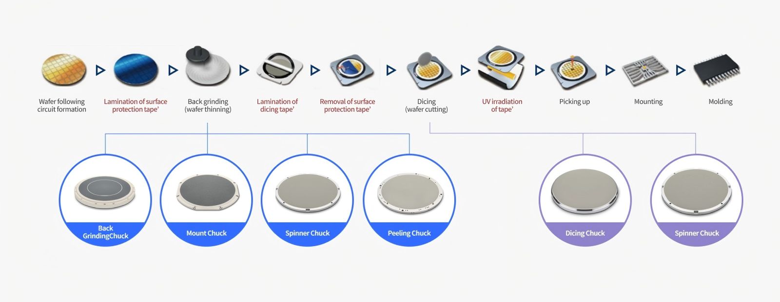
Wafer Chuck vs. Chuck Table – Understanding the Difference
While both are "chucks" in the semiconductor world, wafer chucks and chuck tables serve distinctly different purposes in the manufacturing flow:
Wafer Chuck (Front-End Processing)
-
Purpose: Hold wafers during fabrication processes (lithography, etch, deposition, etc.)
-
Precision: Nanometer-scale flatness and positioning
-
Environment: Cleanroom, often in vacuum or controlled atmosphere
-
Holding Method: Electrostatic or vacuum, full-surface contact
-
Temperature Control: Active heating/cooling systems
-
Key Manufacturers: YICHOU, Creative Technology Corporation, NGK Insulators
Chuck Table (Back-End Processing)
-
Purpose: Hold wafers or substrates during dicing (cutting into individual chips)
-
Precision: Micrometer-scale positioning
-
Environment: Less stringent cleanroom requirements
-
Holding Method: Typically vacuum through porous ceramic
-
Temperature Control: Usually passive
-
Motion: Often rotates or translates during cutting
-
Key Feature: Damage resistance from cutting processes
The Manufacturing Workflow Connection:
-
Front-End: Wafer chucks hold wafers during transistor fabrication
-
Back-End: After processing, wafers move to packaging facilities
-
Dicing: Chuck tables hold wafers while saws or lasers cut individual dies
-
Testing: Modified chucks handle singulated chips during final testing
This distinction highlights how "chuck" technology adapts to different precision requirements throughout the semiconductor lifecycle. YICHOU serves both markets with specialized designs for each application, recognizing that a one-size-fits-all approach cannot meet the divergent needs of front-end fabrication versus back-end packaging.
How Does a Wafer Chuck Work? – Types and Mechanisms
Understanding wafer chuck technology requires diving into the physics and engineering behind these precision devices:
Electrostatic Chucks (ESCs): The Gold Standard
Principle of Operation:
ESCs use the Coulomb force generated by an electrostatic field to hold wafers. When voltage is applied to electrodes embedded in the chuck, opposite charges accumulate on the wafer surface, creating an attractive force that can exceed 1,000 kg/m².
Types of ESCs:
-
Johnsen-Rahbek (J-R) ESCs:
-
Use a semi-insulating layer
-
Develop strong holding forces at relatively low voltages (200-1000V)
-
Faster chucking/dechucking times
-
Preferred for many plasma processes
-
-
Coulombic ESCs:
-
Use a perfect insulator layer
-
Require higher voltages (1000-5000V)
-
More consistent performance over temperature ranges
-
Common in lithography and inspection tools
-
Advanced Features in Modern ESCs:
-
Segmented Electrodes: Allow zone-based control for wafer flattening
-
Integrated Sensors: Monitor temperature, pressure, and contact
-
Self-Diagnostics: Detect degradation or failure before impacting yield
-
Fast Dechucking: Reverse polarity or AC waveforms for quick release
YICHOU's Innovation: Their latest ESCs incorporate proprietary dielectric materials that offer superior breakdown voltage while minimizing charging effects that can damage sensitive devices.
Vacuum Chucks: Simplicity and Reliability
Operation Principle:
Vacuum chucks create a pressure differential between the front and back of the wafer, using atmospheric pressure (approximately 1 kg/cm² at sea level) to hold wafers securely.
Design Variations:
-
Grooved Chucks: Channels distribute vacuum across the surface
-
Porous Chucks: Entire chuck surface acts as a vacuum distributor
-
Patterned Holes: Precision-drilled arrays for optimized holding
Advantages:
-
No electrical fields that might interfere with processes
-
Simpler construction and control
-
Excellent for conductive and non-conductive wafers alike
Limitations:
-
Not suitable for vacuum process chambers
-
Generally lower holding force than ESCs
-
Potential for particle accumulation in holes
Mechanical and Hybrid Systems
While pure mechanical chucks are rare in front-end processing, hybrid systems combine different principles:
-
Vacuum-assisted mechanical clamps
-
Electrostatic with backup mechanical supports
-
Bernoulli-type non-contact "chucks" for ultra-sensitive surfaces
Materials Science Behind Wafer Chucks
The materials used in wafer chuck construction significantly impact performance:
Ceramic Materials (Most Common):
-
Alumina (Al₂O₃): Good all-around properties, cost-effective
-
Aluminum Nitride (AlN): Excellent thermal conductivity
-
Silicon Carbide (SiC): Superior hardness and plasma resistance
-
Macor®: Machinable ceramic for complex geometries
Metal Components:
-
Stainless Steel: For structural elements
-
Invar: Low thermal expansion for critical dimensions
-
Aluminum: Lightweight structural components
Coatings and Treatments:
-
Anodization: For aluminum parts
-
Plasma Spray: Ceramic coatings on metal substrates
-
Diamond-Like Carbon (DLC): Ultra-hard, low-friction surfaces
YICHOU's Material Advantage: Through strategic partnerships with advanced ceramics manufacturers and in-house material development, YICHOU offers chucks with proprietary material compositions that optimize for specific applications—whether maximizing thermal conductivity for high-power processes or achieving the ultimate in flatness for EUV lithography.
Why Can't We Live Without Semiconductors? – The Bigger Picture
To understand why wafer chuck precision matters, consider what semiconductors enable in our world:
The Digital Foundation
Every modern electronic system depends on semiconductors:
-
Computing: CPUs, GPUs, memory, storage controllers
-
Communications: 5G/6G chips, network processors, RF components
-
Transportation: Automotive sensors, infotainment, autonomous driving systems
-
Healthcare: Medical imaging, diagnostic equipment, implantable devices
-
Energy: Smart grid controllers, power conversion, renewable energy systems
Economic Impact
The semiconductor industry:
-
Represents over $500 billion in annual revenue
-
Enables an estimated $7 trillion in downstream economic value
-
Drives innovation across virtually every sector
-
Is strategically critical for national security and technological sovereignty
The Precision Cascade
Here's how wafer chuck precision propagates through the value chain:
-
Nanometer chuck precision →
-
Accurate transistor fabrication →
-
Higher chip performance and yield →
-
More capable electronic systems →
-
Advanced products and services →
-
Economic growth and technological progress
Without the holding precision provided by advanced wafer chucks, the entire semiconductor industry—and by extension, modern civilization—would operate at dramatically reduced capability. This is why companies like YICHOU invest heavily in chuck technology: they're not just selling components; they're enabling the digital infrastructure of the 21st century.
Industry Insights: Manufacturers & Market Leaders
Wafer Chuck Manufacturing Landscape
The wafer chuck market serves a critical niche within the semiconductor equipment ecosystem:
Key Players:
-
YICHOU: Emerging leader with innovative designs and rapid customization capabilities
-
Creative Technology Corporation (CTC): Long-established player with broad product range
-
NGK Insulators: Materials expertise translating to chuck manufacturing
-
TOTO Ltd: Advanced ceramics applied to semiconductor components
-
Kyocera: Diversified ceramics company with semiconductor solutions
Market Dynamics:
-
High barriers to entry: Requires materials science, precision engineering, and semiconductor process expertise
-
Customization intensive: Each major equipment platform needs specialized chuck designs
-
Quality critical: Single chuck failure can cost millions in lost production
-
Continuous innovation: Each process node advancement requires chuck improvements
YICHOU's Competitive Advantages
As a rising leader in wafer chuck technology, YICHOU distinguishes itself through:
-
Vertical Integration:
-
In-house materials development and testing
-
Complete manufacturing from raw materials to finished assembly
-
Direct control over quality at every stage
-
-
R&D Investment:
-
15% of revenue reinvested in research and development
-
Dedicated chuck technology center with full-scale process emulators
-
Partnerships with leading research universities
-
-
Application-Specific Designs:
-
Not just generic chucks, but optimized designs for:
-
EUV lithography
-
High-power etch processes
-
Advanced packaging applications
-
Compound semiconductor processing
-
-
-
Global Support Network:
-
Technical support centers near major semiconductor hubs
-
Rapid replacement programs for critical applications
-
Local inventory for common chuck types
-
-
Sustainability Focus:
-
Designs for extended lifetime and refurbishment
-
Recyclable materials selection
-
Energy-efficient manufacturing processes
-
The ASML Factor
ASML's dominance in lithography equipment (particularly EUV systems) creates a ripple effect throughout the supply chain. Their tools represent the most demanding environment for wafer chucks, requiring:
-
Unprecedented flatness specifications
-
Compatibility with hydrogen environments
-
Resilience to intense EUV radiation
-
Ultra-clean operation with minimal outgassing
YICHOU has developed ASML-qualified chucks that meet these extraordinary requirements, positioning them as a critical supplier to the lithography ecosystem.
TSMC vs. Samsung Foundry Dynamics
The competition between leading foundries drives chuck technology advancement:
-
TSMC: Emphasizes process integration and yield optimization
-
Samsung: Often first to adopt new materials and techniques
Both require increasingly sophisticated chuck solutions, creating opportunities for innovative suppliers who can address their specific technical challenges.
Future Trends: Where Wafer Chuck Technology is Headed
1. Beyond 2nm Requirements
As semiconductor manufacturing advances below 2nm, wafer chucks face new challenges:
-
Atomic-scale flatness: Requirements approaching single atomic layer precision
-
Quantum effects management: Chuck materials and designs that minimize quantum tunneling impacts
-
Hybrid bonding support: Chuck designs enabling wafer-to-wafer stacking with nanometer alignment
2. Heterogeneous Integration
The rise of chiplets and 3D integration demands chucks that can handle:
-
Thinned wafers: Down to 10μm thickness without distortion
-
Mixed materials: Different CTEs in stacked structures
-
Temporary bonding: Support for carriers and debonding processes
3. AI-Enabled Smart Chucks
Future chucks will incorporate:
-
Embedded sensors: Real-time monitoring of force, temperature, and flatness
-
Machine learning algorithms: Predictive maintenance and adaptive control
-
Self-calibration: Automatic adjustment to maintain specifications
4. Sustainability and Circular Economy
-
Extended lifetimes: Designs that maintain performance through more cycles
-
Refurbishment programs: Certified rebuilds with like-new performance
-
Material recycling: Closed-loop systems for ceramic and metal components
5. New Materials and Processes
-
2D material compatibility: Chucks for graphene, MoS₂, and other 2D semiconductors
-
Photonic integration: Specialized chucks for silicon photonics fabrication
-
Quantum computing: Ultra-stable chucks for qubit manufacturing
YICHOU's Roadmap addresses these trends with dedicated research programs in smart chuck technology, advanced materials for future nodes, and sustainable manufacturing processes.
Conclusion: The Precision Behind Every Chip
In the grand narrative of semiconductor advancement—with its focus on transistor density, power efficiency, and computational power—the wafer chuck plays a quiet but indispensable supporting role. Like the foundation of a skyscraper or the runway for a supersonic jet, it provides the stable platform upon which all other advancements are built.
From the smartphones in our pockets to the supercomputers modeling climate change, from life-saving medical devices to the renewable energy infrastructure of tomorrow, semiconductors enable our modern world. And behind every semiconductor, there's a wafer chuck holding it steady during its creation.
Companies like YICHOU exemplify how specialization and deep expertise in seemingly niche components can have outsized impact on entire industries. By pushing the boundaries of what's possible in wafer chuck technology—achieving ever-greater precision, reliability, and intelligence—they're not just improving a component; they're enabling the next generation of technological progress.
As we look toward the semiconductor future—with its promise of angstrom-scale transistors, quantum computing breakthroughs, and pervasive AI—the humble wafer chuck will continue its silent, essential work: holding the future steady, one nanometer at a time.
About YICHOU: With over two decades of specialization in precision holding solutions for semiconductor manufacturing, YICHOU combines advanced materials science, precision engineering, and deep process understanding to deliver wafer chuck solutions that push the boundaries of what's possible in semiconductor fabrication. From research institutions to high-volume fabs, our chucks enable the precision that powers progress.
.jpg)
GET QUOTE
- Visit our website: https://www.nbyichou.com/
- Email us: [email protected]
- Call us/whatsapp: +86 13355741031
- Chat with us: Live chat support available on our website