Introduction
Germanium wafers are a vital component in today’s high-performance electronic and optoelectronic devices. Known for their excellent carrier mobility and high refractive index, germanium wafers are widely used in infrared optics, solar cells, fiber optics, and advanced semiconductor applications. As the demand for faster, more efficient technology continues to grow, so does the importance of this versatile semiconductor material.
However, not all germanium wafers are created equal. Quality, purity, and precision are critical for achieving optimal performance in demanding applications. Choosing the right supplier ensures consistent quality, reliable specifications, and long-term cost efficiency. At YICHOU, we specialize in supplying premium-grade germanium wafers that meet the stringent requirements of global clients across industries such as aerospace, telecommunications, medical imaging, and renewable energy.
1. Understanding Germanium Wafers
What Are Germanium Wafers?
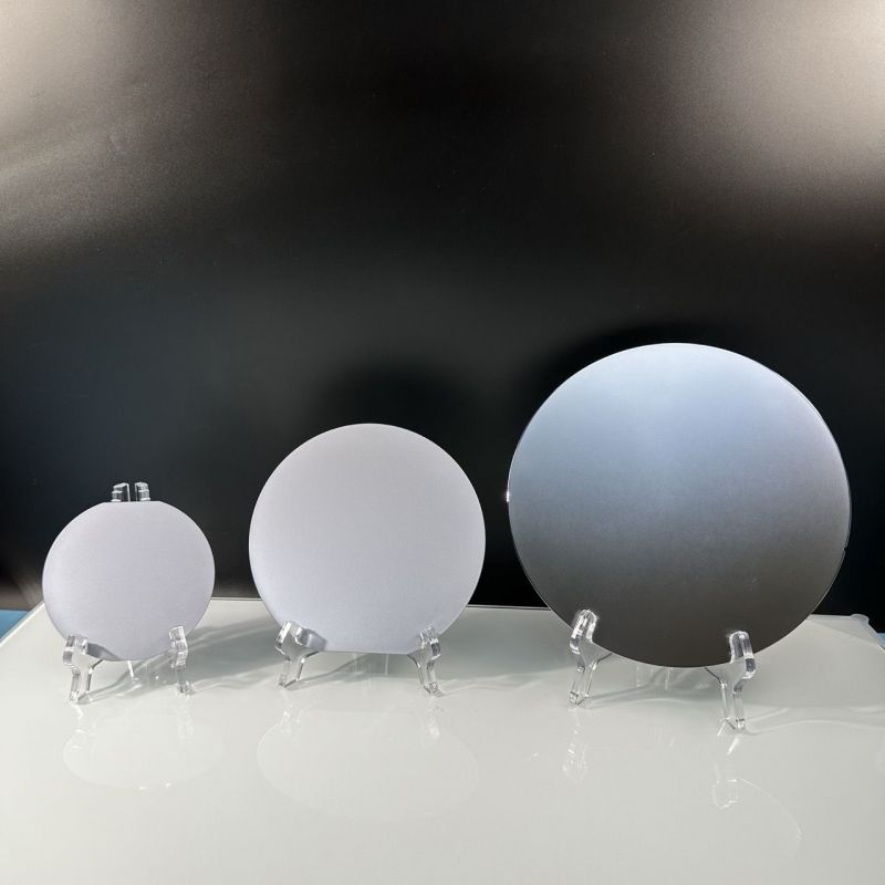
Germanium wafers are thin, circular slices of crystalline germanium used as a semiconductor substrate in the manufacturing of electronic and photonic devices. Germanium (Ge), a Group IV element, offers unique electronic properties—most notably, a high electron and hole mobility—which allow for faster signal processing compared to other semiconductor materials. These wafers are typically produced through zone refining and Czochralski crystal growth, followed by precision slicing and polishing.
Key properties of germanium wafers include:
-
High carrier mobility: Enhances transistor speed and efficiency.
-
Narrow band gap (0.66 eV at room temperature): Ideal for optoelectronic and infrared applications.
-
High refractive index: Beneficial for infrared optics and photodetectors.
-
Excellent surface quality: Supports epitaxial growth for compound semiconductors.
Germanium vs. Silicon: A Material Comparison
While silicon wafers dominate the global semiconductor industry, germanium wafers provide key advantages in niche high-performance applications:
| Property | Germanium | Silicon |
|---|---|---|
| Band Gap | 0.66 eV (narrow) | 1.12 eV (wider) |
| Electron Mobility | ~3900 cm²/V·s | ~1500 cm²/V·s |
| Hole Mobility | ~1900 cm²/V·s | ~450 cm²/V·s |
| Cost | Higher | Lower |
| Availability | Limited | Abundant |
| Applications | Infrared optics, solar cells, high-speed electronics | Microprocessors, memory chips, general-purpose semiconductors |
Although silicon is less expensive and more widely available, germanium’s superior charge carrier mobility and infrared transparency make it the preferred choice for specialized applications such as high-efficiency multi-junction solar cells, infrared optics, and high-speed transistors.
2. Key Applications of Germanium Wafers
Germanium wafers play a pivotal role in advanced technologies across multiple industries due to their exceptional electrical and optical properties. Below are the primary application areas where germanium wafers outperform conventional semiconductor materials.
Infrared Optics
Germanium’s high refractive index and excellent transmission in the infrared (IR) spectrum (2–14 µm range) make it an ideal material for infrared optics. It is widely used in:
-
Thermal imaging cameras
-
Night vision devices
-
Infrared spectrometers
-
Gas analyzers
These wafers are often fabricated into lenses and windows for military, aerospace, and industrial inspection systems. Germanium optics offer superior clarity, sensitivity, and temperature stability under extreme conditions.
Fiber Optics
Germanium is used to dope the core of optical fibers, increasing the refractive index and improving light transmission efficiency. In fiber-optic communication systems, germanium-doped fibers offer:
-
Improved bandwidth
-
Reduced signal loss
-
Higher data transmission rates
This makes germanium a key enabler in high-speed internet, telecommunication backbones, and data centers where performance and stability are critical.
Solar Cells
In the field of photovoltaics, germanium wafers are used as the bottom substrate in multi-junction solar cells, particularly for:
-
Space-based satellites and spacecraft
-
High-efficiency terrestrial solar panels
Multi-junction solar cells that include germanium achieve efficiency levels above 40%, far surpassing traditional silicon cells. The wafer’s ability to handle high radiation and temperature makes it indispensable for aerospace energy systems.
Semiconductor Devices
Thanks to its high electron and hole mobility, germanium is integrated into high-speed and low-power electronic devices such as:
-
Bipolar junction transistors (BJTs)
-
MOSFETs and FinFETs
-
High-frequency and RF integrated circuits
These properties make germanium wafers suitable for next-generation computing, 5G communication devices, and ultra-fast switching systems.

3. Factors to Consider When Purchasing Germanium Wafers
Choosing the right germanium wafer supplier is critical for ensuring device performance, cost-efficiency, and production reliability. Whether you're sourcing wafers for photonics, semiconductors, or solar applications, here are the key factors to evaluate before placing a purchase order.
Purity Levels
High-purity germanium (HPGe) is essential for achieving optimal electrical and optical performance. Impurities can significantly affect the carrier lifetime, conductivity, and overall functionality of the wafer. For most advanced applications, look for:
-
Purity levels of 5N (99.999%) or higher
-
Zone-refined, detector-grade options for infrared and spectroscopy use
-
Low oxygen and carbon content to reduce defect rates
YICHOU provides high-purity germanium wafers manufactured through precision refining processes to meet the strictest industry standards.
Wafer Specifications
Tailoring your wafer specifications to your end application is key to maximizing performance. Common parameters to consider include:
-
Diameter: Standard sizes range from 2 inches (50 mm) to 6 inches (150 mm), depending on application and equipment compatibility.
-
Thickness: Typically ranges from 300 to 800 microns; thinner wafers are used for lightweight or flexible devices.
-
Crystallographic Orientation: ⟨100⟩ or ⟨111⟩ orientation affects doping efficiency, etching behavior, and epitaxial growth.
-
Type and Dopant:
-
N-type: Doped with elements like phosphorus or antimony.
-
P-type: Doped with boron or gallium.
-
At YICHOU, we offer customization for all of these parameters to match your exact technical requirements.
Supplier Credibility
Not all suppliers offer the same level of quality or reliability. When selecting a germanium wafer supplier, ensure they provide:
-
ISO-certified production facilities
-
Batch-level quality control with documentation
-
In-house testing for resistivity, flatness, and defect density
-
On-time delivery and responsive technical support
At YICHOU, we take pride in our quality assurance process, advanced metrology equipment, and strong customer support team that works closely with clients from prototyping to mass production.
4. Market Trends and Supply Chain Insights
As a critical material in next-generation optics, electronics, and renewable energy, germanium wafers are experiencing increasing global demand. However, their market is uniquely sensitive to geopolitical dynamics, making supply chain stability a top concern for procurement teams.
Growing Market Demand
The global germanium wafer market is witnessing sustained growth, driven by sectors such as:
-
Infrared sensing in defense and automotive (ADAS)
-
High-speed optical communication networks
-
High-efficiency multi-junction solar cells used in aerospace
-
Next-gen semiconductors for AI and 5G devices
According to recent industry forecasts, the demand for high-purity germanium wafers is expected to grow at a CAGR of over 7% from 2024–2030, driven largely by space-grade solar and infrared applications.
Geopolitical Factors & Export Restrictions
Germanium is classified as a critical raw material, with the majority of the world’s refined supply originating from a few key countries, especially China.
In 2023, China implemented export controls on gallium and germanium-related materials, citing national security concerns. This led to significant market volatility and heightened global awareness of the supply chain's fragility. Buyers outside of China faced:
-
Longer lead times
-
Price fluctuations
-
Limited access to high-purity stock
Such geopolitical factors have prompted governments and companies to diversify their sourcing and build strategic inventories.
Strategies for Mitigating Supply Chain Risks
Procurement professionals can take several steps to ensure a stable and secure germanium wafer supply:
-
Partner with a Reliable Domestic Supplier
Companies like YICHOU provide vertically integrated production—from raw material sourcing to wafer processing—ensuring consistent quality and availability even during trade restrictions. -
Place Blanket Orders or Long-Term Agreements (LTAs)
Secure supply at fixed pricing by entering longer-term contracts, which also help suppliers plan their production pipeline effectively. -
Dual-Sourcing Strategies
Consider working with multiple suppliers in different countries to reduce regional risk exposure. -
Inventory Buffering
Maintain a rolling inventory of germanium wafers for critical applications to prevent production disruptions.
At YICHOU, we support our clients with flexible sourcing models, transparent lead times, and stable pricing policies—backed by a robust export infrastructure that continues to ship worldwide.
5. Why Choose YICHOU for Your Germanium Wafer Needs
When it comes to sourcing high-quality germanium wafers, YICHOU stands out as a trusted, innovative, and responsive supplier for customers worldwide.
Proven Industry Expertise
With years of experience in precision materials processing and semiconductor-grade wafer manufacturing, YICHOU has developed deep technical know-how and strong production capabilities. We serve industries including:
-
Infrared optics and defense
-
Aerospace solar technologies
-
Optical communications
-
Advanced semiconductors and photonics
Our engineers work closely with clients to optimize performance and ensure every wafer meets project-specific standards.
Customization & Quality Assurance
Every application is different—and so is every wafer we produce. At YICHOU, we offer:
-
Custom doping (N-type or P-type)
-
Orientation control (⟨100⟩ or ⟨111⟩)
-
Precise thickness, diameter, and surface finish
-
Ultra-high purity options (up to 6N)
Each wafer undergoes strict in-house inspection, including resistivity testing, flatness analysis, and surface defect screening. We are ISO-certified and maintain full traceability throughout the production process.
Trusted by Global Clients
YICHOU’s commitment to excellence has earned us long-term relationships with clients across North America, Europe, and Asia.
Case Study: A U.S. aerospace company required custom-sized, radiation-hardened germanium wafers for their satellite solar panels. YICHOU delivered a high-yield batch within 21 days—fully documented, precision-tested, and exceeding purity expectations. The client has since expanded to quarterly volume orders.
Conclusion
In a rapidly evolving technology landscape, selecting the right germanium wafer supplier is more than a procurement decision—it’s a strategic advantage. From ensuring product performance to securing long-term supply, every detail matters.
YICHOU is your dependable partner for germanium wafer sourcing, offering unmatched quality, customization, and technical support. Whether you need prototyping quantities or mass production, we are ready to support your success.
Call to Action
Ready to source high-performance germanium wafers?
.jpg)
GET QUOTE
- Visit our website: https://www.nbyichou.com/
- Email us: [email protected]
- Call us/whatsapp: +86 13355741031
- Chat with us: Live chat support available on our website