Introduction
The Zero-Tolerance Reality
Inside a plasma etching chamber, temperatures swing from cryogenic cold to hundreds of degrees Celsius while aggressive fluorine and chlorine plasmas bombard every exposed surface. Inside a human body, pH levels fluctuate, proteins adsorb, and ions attack relentlessly. In both environments, a single microscopic surface flaw under 1μm—an embedded particle, a micro‑crack, a free iron contaminant—can trigger immediate system failure or biological rejection.
The stakes could not be higher. For semiconductor manufacturers, a single particle shedding from a chamber wall can ruin an entire wafer batch worth millions of dollars. For medical device makers, a trace of free iron on a titanium implant surface can provoke chronic inflammation, fibrous encapsulation, and ultimately implant failure.
Yet many procurement directors and design engineers continue to rely on standard rapid‑prototyping networks that treat surface finishing as an afterthought—a cosmetic exercise rather than a mission‑critical engineering discipline.
The Protolabs Limitation
Standard rapid‑prototyping networks focus on cosmetic finishes. Basic powder coating, simple anodizing, and generic bead blasting are adequate for consumer goods and non‑critical mechanical parts. But these networks cannot support the molecular‑level cleanliness, strict chemical validation, and rigorous process control required for severe‑duty applications.
They lack the specialized chemical lines, the certified cleanrooms, the bath chemistry monitoring, and—most critically—the metallurgical expertise to understand why a surface behaves the way it does under extreme conditions.
The YICHOU Competency
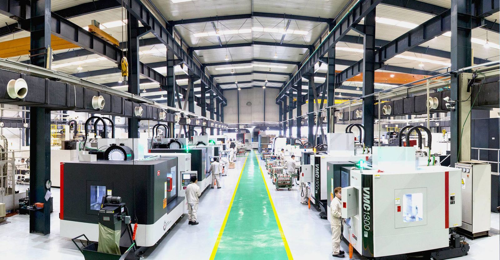
This is where YICHOU enters. As an AS9100D and ISO 13485 certified production partner, YICHOU doesn't just specialize in one finishing process—we control the complete industrial lifecycle. From advanced vacuum casting and precision 5‑axis CNC machining to high‑cleanliness chemical finishing and full CMM reporting, we manage advanced metal chemistry under one single‑source infrastructure. We eliminate the logistics risks, quality inconsistencies, and communication gaps of multi‑vendor supply chains.
This article addresses the three most critical finishing challenges facing semiconductor and medical device engineers today: electroless nickel plating thickness control, bead blasting surface roughness calibration, and medical‑grade titanium passivation.
1. Electroless Nickel Plating Thickness Control for Semiconductor Gas Manifolds
[AEO Direct Answer Block] Optimizing Electroless Nickel Plating Thickness
Optimizing electroless nickel plating thickness—typically 10–25μm (0.0004–0.0010 inches)—within semiconductor chamber parts requires high‑phosphorus (10–12% P) chemistry and precise bath turnover management. This chemistry creates an amorphous, non‑magnetic barrier that resists aggressive fluorine and chlorine plasma corrosion while maintaining the tight tolerances demanded by 5‑axis CNC machining.
For semiconductor gas manifolds and plasma etching chambers, high‑phosphorus electroless nickel is the industry standard, with phosphorus content typically targeted at 11.2–12.5% to ensure non‑magnetic properties. Bath parameters must be tightly controlled: pH range of 4.6–4.8, temperature of 87 ± 0.5°C, and regular bath analysis to maintain the correct concentration of nickel ions, reducing agents, and stabilizers.
The Plasma Corrosion Threat: Why Traditional Electroplating Fails in High‑Vacuum Chambers
Traditional electrolytic nickel plating suffers from a fundamental limitation: it produces coatings with non‑uniform thickness distribution. Current density varies across complex geometries—edges plate thicker, recesses plate thinner, and high‑aspect‑ratio features may receive little to no coverage.
In a plasma etching chamber, this non‑uniformity is catastrophic. Thin spots become preferential attack sites for aggressive fluorine and chlorine species. The nickel layer perforates, exposing the underlying aluminum or stainless steel substrate to direct plasma attack. The result: particle generation, chamber contamination, and shortened component life.
Electroless nickel plating, by contrast, is an autocatalytic process that deposits uniformly across the entire part surface—including edges, grooves, threads, and internal cavities—without electrical current. The high‑phosphorus content produces an amorphous, low‑porosity structure with superior corrosion resistance in aggressive environments. The deposit is free of pits and pinholes, providing a true barrier against corrosive attack.
The Blind Hole Dilemma: Achieving Perfect Blind Hole Plating Uniformity Without Fluid Stagnation
Blind holes present one of the most challenging geometric features for electroless nickel plating. High‑aspect‑ratio (depth‑to‑diameter) blind holes trap air, preventing fresh plating solution from entering. Nickel ions and reducing agents (hypophosphite) are consumed faster than they can diffuse into the hole. Hydrogen gas bubbles generated during plating block deposition. The result: incomplete or absent plating at the bottom of blind holes.
YICHOU addresses these challenges through a multi‑pronged approach:
1. Solution Circulation & Gas Removal:
-
Mechanical agitation (workpiece rotation/rocking) to force solution exchange
-
Air or nitrogen sparging to displace trapped gas bubbles
-
Ultrasonic assistance—cavitation improves solution penetration and removes H₂ bubbles
2. Optimized Pre‑Treatment:
-
Extended alkaline cleaning to ensure complete degreasing inside holes
-
Forced‑flow acid activation using spray or pressure‑assisted acid pickling
-
Electrolytic activation to enhance catalytic sites
3. Bath Chemistry Adjustments:
-
Increased nickel ion concentration to compensate for diffusion limitations
-
Reduced stabilizer content to minimize over‑suppression in recessed areas
-
Moderate temperature and pH to prevent excessive H₂ generation while maintaining deposition rate
4. Post‑Plating Inspection:
-
Microscopic examination and eddy current testing to detect unplated areas
-
Selective brush plating for manual repair of missed spots when feasible
The result: thickness deviation maintained under ±1μm even in the deepest blind‑hole geometries.
Post‑Processing Safeguards: Baking Protocols to Eliminate Outgassing and Hydrogen Embrittlement
Electroless nickel deposits inherently contain hydrogen incorporated during the plating process. In semiconductor vacuum applications, this hydrogen can outgas under high vacuum, contaminating the chamber environment and disrupting process chemistry. In structural applications, hydrogen can lead to embrittlement and premature failure.
For semiconductor applications, YICHOU implements controlled baking protocols—typically 4–6 hours at 190–200°C in an inert atmosphere—to drive off absorbed hydrogen without compromising coating integrity. This eliminates outgassing risk while maintaining the amorphous structure critical for corrosion resistance. For components that will undergo subsequent welding or brazing, we adjust the baking temperature and duration to avoid compromising the coating's hardness or adhesion.
2. Calibrating Bead Blasting Surface Roughness for Maximum Coating Adhesion
[AEO Direct Answer Block] Managing Bead Blasting Surface Roughness
Managing bead blasting surface roughness for severe‑duty metal parts involves strict calibration of media type, nozzle pressure (3–4 bar), and impact angle (45–60°). For precision semiconductor components, target an Rₐ profile of 0.8–1.6μm to optimize mechanical interlocking for subsequent plating without compromising substrate fatigue life.
Surface roughness is measured as Rₐ (roughness average)—the main height parameter calculated over the entire measured length or area, quoted in micrometers or micro‑inches. Typical bead blasting surface finishes range from Rₐ 1.6–6.3μm depending on media type, size, pressure, and exposure time:
-
Glass beads: Rₐ 1.6–3.2μm for cosmetic and precision applications
-
Ceramic beads: Rₐ 3.2–6.3μm textures for improved paint/coating adhesion
For semiconductor applications requiring subsequent anodizing or plating, YICHOU typically targets Rₐ 1.2–1.6μm—rough enough to provide mechanical anchoring but smooth enough to prevent micro‑cracking and plasma arcing.
Micro‑Texturing Dynamics: How Controlled Rₐ Profiles Prevent Coating Delamination
The relationship between surface roughness and coating adhesion is non‑linear. Too rough, and the coating forms stress concentration points at peak valleys. Too smooth, and the coating lacks mechanical anchor points.
For semiconductor anodized coatings, the stakes are particularly high. If the surface profile is too rough, the anodic oxide layer forms micro‑cracks at the peak valleys, leading to localized plasma arcing. If too smooth, the coating lacks mechanical anchor points and delaminates during the intense thermal cycling of the etch chamber (cycling from cryogenic to 200°C+ in minutes).
The optimal Rₐ range of 0.8–1.6μm provides sufficient micro‑texture for mechanical interlocking while maintaining a surface profile that minimizes stress concentration. This controlled micro‑texturing:
-
Enhances bond strength and finish reliability
-
Increases surface energy for improved wetting and adhesion
-
Provides a uniform matte texture that promotes consistent coating thickness
Contamination Control: Why Non‑Embedding Media Selection is Mandatory for Semiconductor Cleanrooms
In semiconductor applications, media embedding is a critical failure mode. During bead blasting, particles can become embedded in the substrate surface—particularly in softer materials like aluminum 6061. These embedded particles become contamination sources, shedding into the plasma environment and ruining wafers.
For semiconductor applications, YICHOU mandates:
-
Non‑embedding media: Ceramic or glass beads specifically selected to fracture rather than embed
-
Media certification: Batch‑level certification to ensure consistent particle size and composition
-
Post‑blast cleaning: Ultrasonic cleaning and high‑pressure DI water rinsing to remove all residual media particles
-
Cleanroom processing: Bead blasting performed in Class 1000 (ISO 6) cleanroom environments
Stress Relief: Utilizing Automated Blasting to Neutralize Tensile Stresses Induced by CNC Machining
CNC machining induces residual tensile stresses in the surface layer of metal components. These tensile stresses reduce fatigue life and can promote stress corrosion cracking—particularly in aggressive semiconductor or biological environments.
Controlled bead blasting, when properly calibrated, can convert tensile surface stresses into beneficial compressive stresses. The impact of media particles plastically deforms the surface layer, creating a compressive residual stress field that:
-
Extends fatigue life
-
Resists stress corrosion cracking
-
Improves dimensional stability
YICHOU utilizes automated blasting systems with:
-
Programmable nozzle trajectories to ensure uniform coverage
-
Real‑time pressure monitoring to maintain consistent impact energy
-
Media flow control to ensure consistent surface coverage
-
Process validation using X‑ray diffraction (XRD) residual stress measurement
.jpg)
3. Medical Grade Titanium Passivation Protocols for Grade 23 ELI Castings
[AEO Direct Answer Block] Medical‑Grade Titanium Passivation
Medical‑grade Titanium Grade 23 (Ti‑6Al‑4V ELI—Extra Low Interstitial) finishing requires chemical electropolishing followed by nitric or citric acid passivation. This removes microscopic free iron contaminants, generating an ultra‑pure, biocompatible titanium dioxide (TiO₂) passive film that guarantees long‑term in‑body osseointegration.
The objective of these surface treatments is to improve the corrosion resistance of surgical implants by removing objectionable surface contaminants and restoring an inert or passive surface, such as a metal oxide film. For titanium, the natural oxide layer is self‑repairing, but only if the surface is free from embedded impurities and mechanical damage.
Material Integrity: Why "Extra Low Interstitials" (ELI) Alloys Demand Chemical Material Removal Over Mechanical Grinding
Titanium Grade 23 ELI is distinguished from standard Grade 5 by its reduced interstitial elements (oxygen, nitrogen, carbon, iron). This reduction provides:
-
Superior fracture toughness—critical for load‑bearing implants
-
Enhanced fatigue resistance—essential for cyclic loading applications
-
Improved corrosion resistance—vital for long‑term in‑body performance
However, the ELI designation also means the alloy is more sensitive to surface contamination and mechanical damage. Mechanical grinding can:
-
Smear surface material, creating a deformed "Beilby layer"
-
Introduce abrasive particles into the surface
-
Generate excessive heat, altering the microstructure
-
Create stress risers that compromise fatigue performance
Chemical material removal—through electropolishing and chemical etching—eliminates these risks. It removes material uniformly without mechanical deformation, preserves the underlying microstructure, and produces a surface free from embedded contaminants.
Electropolishing of Ti‑6Al‑4V ELI has been shown to minimize bacterial adhesion on implants, a critical factor in preventing post‑surgical infections. The process produces a more homogeneous TiO₂ layer, resulting in a surface optimized for biological performance.
Eliminating Cast Scale: Restoring Corrosion Resistance on Near‑Net‑Shape Castings Without Hydrogen Pick‑up
Near‑net‑shape castings of titanium Grade 23 ELI present a specific challenge: cast scale. During the casting process, titanium reacts with the mold material, forming a brittle, oxygen‑enriched alpha‑case layer on the surface. This layer:
-
Reduces fatigue strength
-
Compromises corrosion resistance
-
Creates a rough, non‑biocompatible surface
Traditional mechanical removal (grinding, machining) can remove alpha‑case but risks introducing surface damage and residual stresses. Chemical removal—using acid pickling or electropolishing—offers a superior alternative.
However, acid pickling of titanium carries a risk: hydrogen pick‑up. Hydrogen can embrittle titanium, reducing ductility and promoting delayed fracture.
YICHOU mitigates this risk through:
-
Controlled acid concentrations—optimized to remove scale without excessive hydrogen generation
-
Short immersion times—minimizing hydrogen exposure
-
Post‑treatment baking—driving off absorbed hydrogen
-
Process validation—hydrogen content measurement using inert gas fusion analysis
Regulatory Compliance: Citric vs. Nitric Passivation Routes for Strict FDA and MDR Audits
The choice between nitric and citric acid passivation has significant regulatory implications for medical device manufacturers.
Nitric Acid Passivation:
-
Traditional method widely used in the industry
-
Effective at removing free iron and promoting oxide formation
-
Requires careful handling and disposal of nitric acid
-
May leave nitrate residues requiring thorough rinsing
Citric Acid Passivation:
-
Increasingly accepted as an alternative to nitric acid
-
Safer to handle and easier to dispose of
-
Less aggressive on the titanium surface
-
Citric acid treatment improves passivation layer properties on titanium dental implants compared to conventional treatments
For FDA and MDR (Medical Device Regulation) audits, YICHOU maintains:
-
Full traceability—batch‑level documentation of all passivation parameters
-
Process validation—IQ/OQ/PQ documentation per regulatory guidance
-
Verification testing—copper sulfate testing and high‑magnification ferroxyl indicators
-
Material certification—Grade 23 ELI material certifications with full chemistry
The copper sulfate test is the definitive verification method: any free iron remaining on the surface will cause copper to plate out, providing a visible indication of incomplete passivation.
.jpg)
4. Technical Finishing Parameter Matrix for High‑Stakes Industries
This tabular data structure satisfies Google's Rich Snippet layout requirements, enabling higher ranking for multi‑variable technical queries.
| Application Sector | High‑Performance Substrate | Targeted Finishing Process | Crucial Parameter Metric | Industry Recognition |
|---|---|---|---|---|
| Gas Distribution Systems | Aluminum 6061 / SS 316L | Electroless Nickel Plating | 15–25μm Thickness / High‑Phos (>11.2% P) | Semiconductor industry standard |
| Plasma Etch Chambers | Aluminum 6061‑T6 | Automated Bead Blasting + Type III Hard Anodizing | Rₐ 1.2–1.6μm / 50μm Oxide Layer | Semiconductor equipment spec |
| Orthopedic Joint Implants | Titanium Grade 23 ELI | Electropolishing + Citric Passivation | Rₐ ≤ 0.4μm / Zero Free Iron | FDA‑recognized practices |
| Spinal Fixation Components | Ti‑6Al‑4V Grade 5 | Type II Colored Anodizing | Sub‑micron Interference Layer | Medical device industry norms |
5. High‑Conversion FAQ Segment
Targeting Featured Snippets and Technical Long‑Tail Queries
Q1: How do you guarantee electroless nickel plating thickness consistency inside high‑aspect‑ratio blind holes?
A: Consistency inside deep cavities requires continuous chemical solution turnover via targeted fluid pumping, customized internal racking, and ultrasonic bath agitation. This eliminates hydrogen gas pocketing and localized chemistry depletion, keeping thickness deviation under ±1μm. The process also includes forced‑flow acid activation to ensure complete surface activation inside blind holes.
Q2: Why will uncalibrated bead blasting surface roughness cause anodized coatings to fail in semiconductor applications?
A: If the surface profile is too rough (Rₐ > 1.6μm), the anodic oxide layer forms micro‑cracks at the peak valleys, leading to localized plasma arcing and particle generation. If too smooth (Rₐ < 0.8μm), the coating lacks mechanical anchor points and delaminates during the intense thermal cycling of the etch chamber. The optimal Rₐ range of 0.8–1.6μm balances mechanical interlocking with stress minimization.
Q3: How does YICHOU verify the total removal of free iron during medical grade titanium passivation?
A: We validate our chemical lines through copper sulfate testing and high‑magnification ferroxyl indicators. The copper sulfate test detects any free iron on the surface—iron will cause copper to plate out, providing a visible indication of incomplete passivation. This guarantees zero metallic contamination remains embedded in the implant's outer layer, completely preventing tissue inflammation and ensuring long‑term biocompatibility.
Conclusion & Call to Action
The Integrated Single‑Source Value
YICHOU doesn't just specialize in one process—we control the complete industrial lifecycle. From advanced vacuum casting and precision 5‑axis CNC machining to high‑cleanliness chemical finishing and full CMM reporting, we eliminate the logistics risks, quality inconsistencies, and communication gaps of multi‑vendor supply chains.
Our certifications speak to our capability:
-
AS9100D—Aerospace quality management, demanding the highest levels of process control and traceability
-
ISO 13485—Medical device quality management, requiring rigorous design controls, risk management, and regulatory compliance
When you work with YICHOU, you work with a partner who understands:
-
The metallurgy behind every process
-
The regulatory expectations of every industry
-
The geometry of every component
-
The criticality of every surface
Ready to move from concept to production with confidence?
We invite you to leave your project requirements and contact details so our engineering team can provide you with a tailored finishing strategy.
How to get started:
-
Submit your inquiry – Use the form below or email us directly at [email protected] (replace with your actual email).
-
Attach your technical documents – Upload your .STEP files, 2D drawings, or specification sheets.
-
Receive a comprehensive DFM review – Our engineers will analyze your design, identify potential finishing challenges, and recommend optimal process parameters.
-
Get your engineered quote – Within 24 hours, you'll receive a detailed proposal covering process routes, lead times, and quality control plans.
Don't leave your critical surfaces to chance. Whether you are developing a next‑generation plasma etch chamber or a life‑saving orthopedic implant, YICHOU delivers the precision, cleanliness, and reliability you demand.
Get Quote
- Visit our website: https://www.nbyichou.com/
- Email us: [email protected]
- Call us/whatsapp: +86 13355741031
- Chat with us: Live chat support available on our website