Maximizing Wafer Yield:
Overcoming Thermal Stress and Chemical Erosion in MOCVD and Epitaxial Growth Processes
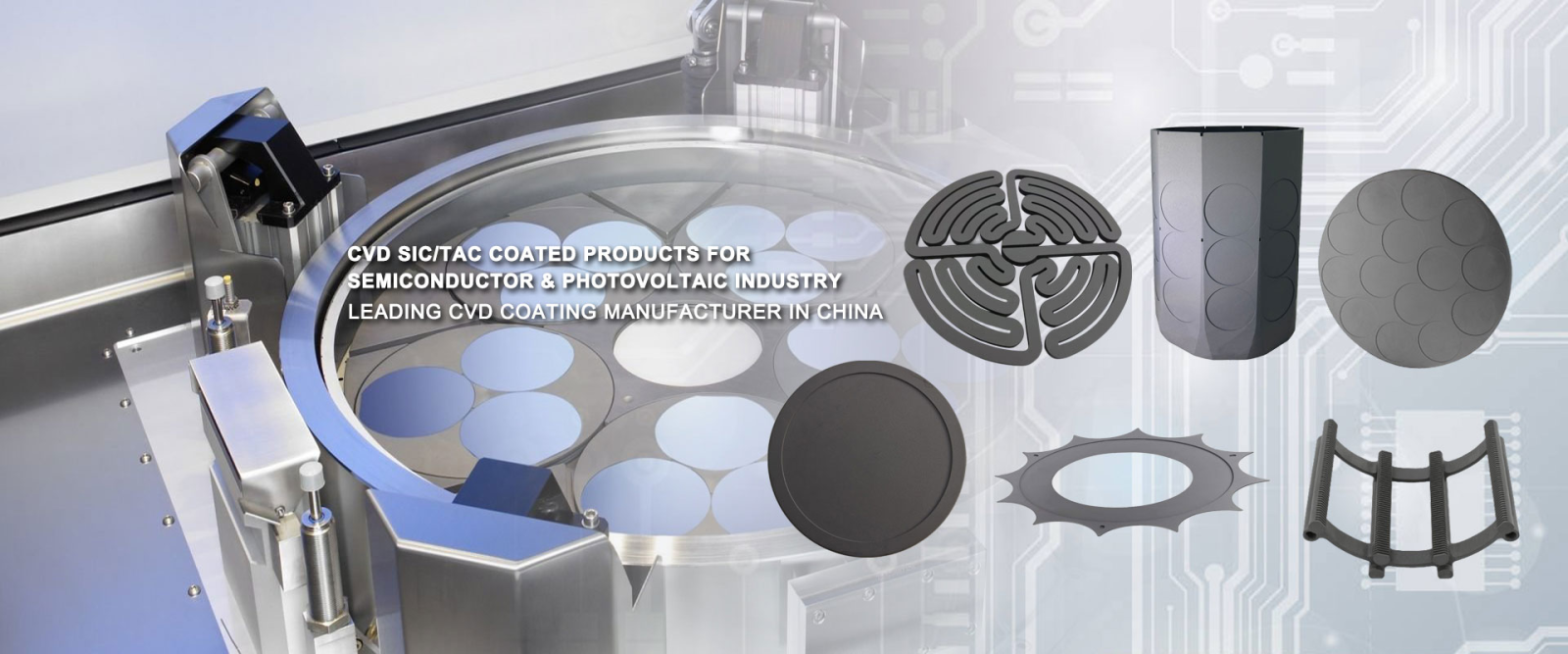
Brand Focus: YICHOU Precision Machining (www.nbyichou.com)
1. Introduction: The Critical Role of Susceptors in Semiconductor Fabrication
In the intricate world of semiconductor manufacturing, some components remain hidden from view yet determine the success or failure of the entire fabrication process. The wafer susceptor—also known as the wafer carrier—is precisely such a component. At first glance, it appears to be little more than a specialized tray that holds wafers during processing. However, this perception couldn't be further from the truth. The susceptor is, in reality, a sophisticated thermal management tool that operates at the intersection of materials science, precision engineering, and process chemistry.
The fundamental question that every semiconductor engineer asks is simple: What is a SiC susceptor, and why does it matter? The answer lies in its function. During Metal-Organic Chemical Vapor Deposition (MOCVD) and epitaxial growth processes—particularly for wide-bandgap semiconductors like Gallium Nitride (GaN) and Silicon Carbide (SiC)—the susceptor serves as the platform upon which single-crystal thin films are grown. It must provide an ultra-pure, thermally uniform, and mechanically stable surface while withstanding temperatures that would destroy ordinary materials.
The stakes couldn't be higher. A susceptor that introduces temperature variations of just a few degrees across its surface can render an entire batch of wafers unusable due to non-uniform epitaxial layer thickness. Contamination from the susceptor material can destroy the delicate electronic properties that make wide-bandgap semiconductors valuable. In an industry where a single 200mm wafer can be worth thousands of dollars, the economic impact of susceptor performance—or failure—is enormous.
At YICHOU Precision Machining, we have made it our mission to engineer the next generation of semiconductor-grade graphite and SiC carriers. Our approach combines decades of precision machining experience with cutting-edge materials science to produce components that meet the exacting demands of modern semiconductor fabs. This comprehensive guide explores the engineering excellence behind CVD SiC coated susceptors and provides actionable insights for professionals seeking to maximize wafer yield and process reliability.
2. Material Science: Why CVD SiC Coating is Non-Negotiable
The Base Material: High-Purity Isostatic Graphite
Every exceptional susceptor begins with an exceptional foundation. At YICHOU, we start with high-purity isostatic graphite—a material specifically engineered for semiconductor applications. The term "isostatic" refers to the manufacturing process, where graphite powder is compressed under equal pressure from all directions, resulting in a material with uniform properties in every orientation.
The purity requirements for semiconductor-grade graphite are staggering. We specify graphite with purity levels exceeding 99.9999% (six nines), meaning that the total concentration of metallic impurities is measured in parts per billion (ppb) rather than parts per million. Why such extreme purity? Because at the operating temperatures of MOCVD reactors—typically between 1000°C and 1600°C—impurities can migrate from the graphite to the wafer surface, where they act as recombination centers that degrade device performance.
Isostatic graphite offers several additional advantages that make it the material of choice for susceptor bases:
-
Excellent thermal conductivity: Ensures rapid heat transfer to the wafer
-
Low thermal mass: Allows for quick temperature changes during processing
-
Machinability: Can be shaped to precise tolerances before coating
-
Thermal shock resistance: Withstands the rapid temperature ramps common in epitaxial growth
The Protective Layer: CVD Silicon Carbide Coating
While high-purity graphite provides an excellent foundation, it cannot survive unprotected in the harsh environment of an MOCVD reactor. The process gases used in epitaxial growth—including hydrogen (H₂), ammonia (NH₃), and various chlorine-containing compounds—would rapidly attack bare graphite, causing erosion and particle generation. This is where Chemical Vapor Deposition (CVD) Silicon Carbide coating becomes essential.
The CVD process for SiC coating involves introducing silicon-containing and carbon-containing gases into a high-temperature reaction chamber. At temperatures typically exceeding 1000°C, these gases decompose and react on the surface of the graphite substrate, forming a dense, uniform layer of crystalline silicon carbide. The result is a coating with remarkable properties:
Crystal Structure: The CVD process produces beta-phase silicon carbide (β-SiC) with a cubic crystal structure. This phase is preferred for semiconductor applications due to its high purity and excellent mechanical properties.
Density: At 3.21 g/cc, CVD SiC achieves near-theoretical density with zero porosity. This eliminates pathways for corrosive gases to reach the underlying graphite.
Hardness: With a Vickers hardness of 2500-2800, CVD SiC is second only to diamond in hardness. This exceptional wear resistance ensures that the susceptor surface remains pristine through countless processing cycles. Under optimized deposition conditions, hardness values exceeding 42 GPa can be achieved for preferentially oriented 3C-SiC coatings.
Chemical Purity: The CVD process naturally produces material of extraordinary purity. Our CVD SiC coatings achieve impurity levels so low they challenge the limits of detection equipment.
Thermal Properties: The coating exhibits thermal conductivity of 300 W/mK and a coefficient of thermal expansion (CTE) carefully matched to the underlying graphite.
Recent advances in precursor chemistry have enabled even more refined control over the CVD process. The use of chlorine-free organosilane compounds, such as polysilaethylene (PSE), offers significant advantages including lower deposition temperatures, faster deposition rates, and elimination of corrosive by-products. This approach represents the next generation of environmentally friendly SiC coating technology.
The CTE Matching Challenge
One of the most critical aspects of susceptor engineering is matching the coefficient of thermal expansion between the graphite base and the SiC coating. If these materials expand at different rates during the extreme temperature cycles of epitaxial growth, the coating can delaminate or crack—a catastrophic failure that contaminates the entire reactor.
Graphite typically has a CTE of 4-6 × 10⁻⁶/K in the plane of the susceptor, while bulk SiC has a CTE of approximately 4.5 × 10⁻⁶/K. Through careful selection of graphite grades and optimization of the CVD process, YICHOU achieves a near-perfect CTE match that prevents delamination even after thousands of thermal cycles. This engineering achievement is the result of extensive research and development, combined with rigorous testing protocols that verify coating integrity before any product leaves our facility.
| Property | Uncoated Graphite | Standard SiC Coating | YICHOU Semiconductor-Grade CVD SiC |
|---|---|---|---|
| Purity | 99.9% - 99.99% | 99.99% - 99.999% | >99.9999% |
| Density (g/cc) | 1.7 - 1.9 | 3.20 - 3.21 | 3.21 (theoretical) |
| Hardness (GPa) | <1 | 20 - 30 | >42 (optimized) |
| Porosity | 10% - 15% | <1% | Zero (hermetic) |
| Max Operating Temp (°C) | 500 (oxidizing) | 1400 (oxidizing)/1600 (inert) | 1600°C continuous |
| CTE Match to Graphite | N/A | Good | Near-perfect |
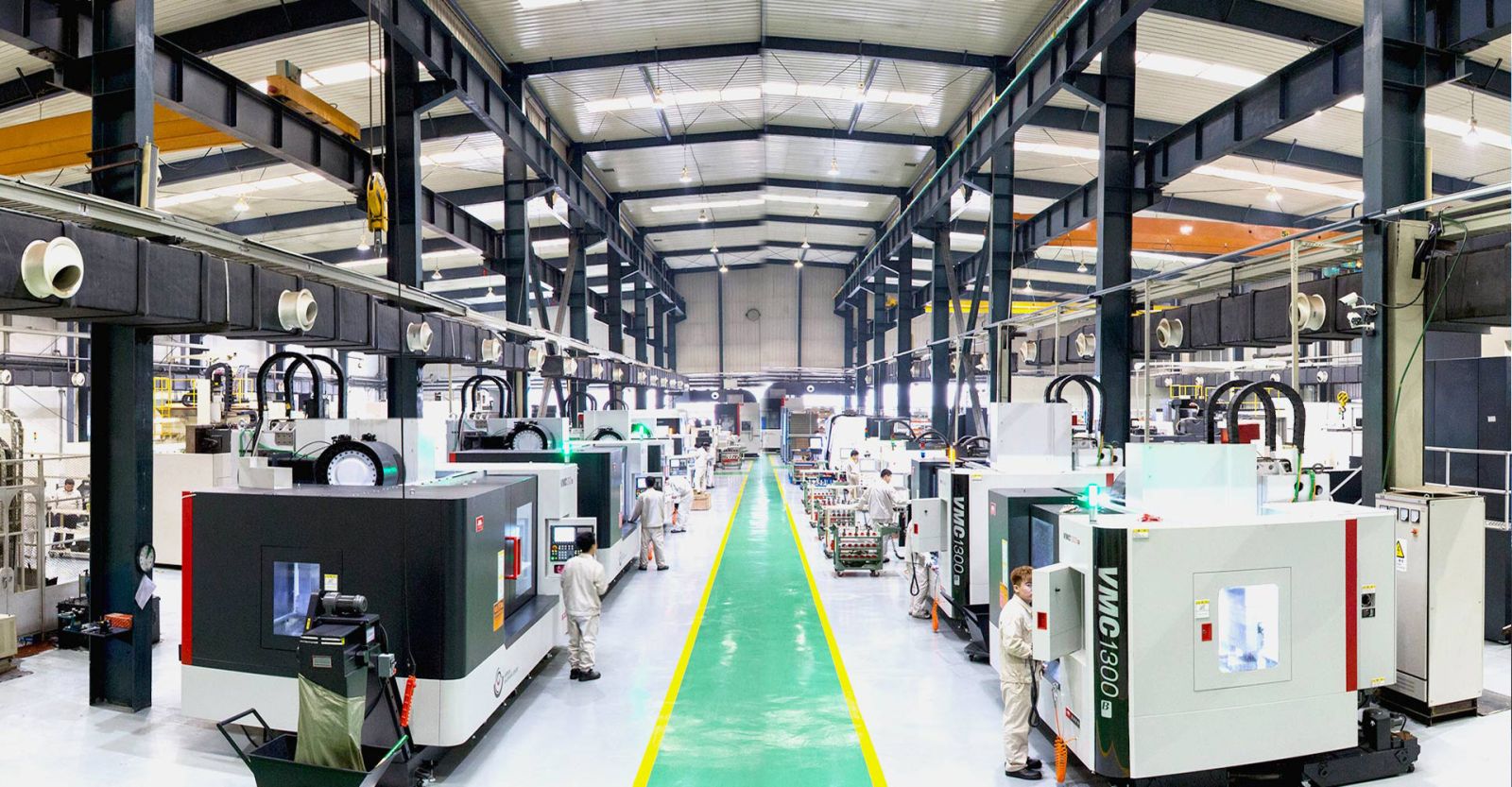
3. Precision Engineering: Achieving Sub-Micron Pocket Accuracy
The Challenge of Machining SiC
If silicon carbide coating is essential for chemical protection, precision machining is equally critical for process performance. The pockets that hold wafers in the susceptor must maintain dimensional tolerances measured in microns—or even fractions of microns—to ensure proper wafer seating and uniform heating.
The challenge is that silicon carbide is extraordinarily difficult to machine. With hardness second only to diamond, conventional cutting tools are useless against CVD SiC. This is why standard CNC shops cannot produce semiconductor-grade susceptors, regardless of their experience with other materials.
YICHOU's Advanced Machining Capabilities
At YICHOU, we have invested in specialized machining technologies capable of working with ultra-hard materials:
Ultrasonic Grinding: This technique combines high-frequency vibration with diamond abrasive to remove material from the SiC surface. The ultrasonic action reduces cutting forces and allows for precise control of material removal rates, enabling the creation of pocket geometries that would be impossible with conventional methods.
Diamond Micro-Machining: For the finest features and smoothest surfaces, we employ diamond tooling in ultra-precision machining centers. These machines operate in temperature-controlled environments to eliminate thermal expansion effects during machining, achieving tolerances that push the limits of what's physically possible.
Pocket Uniformity Requirements
The wafer pockets in a susceptor must meet specifications that seem almost impossibly tight to those outside the semiconductor industry:
Flatness: The bottom of each pocket must be flat to within <10 μm across the entire pocket diameter. Any deviation from flatness translates directly into temperature non-uniformity in the wafer, which in turn causes variations in epitaxial layer thickness.
Depth Control: Pocket depth must be held to tolerances of ±0.005 mm (5 microns). If a pocket is too shallow, the wafer will sit proud of the surface, disrupting gas flow patterns. If too deep, the wafer may not contact the susceptor properly, leading to poor heat transfer.
Surface Roughness: The pocket surface must achieve a mirror-like finish with roughness (Ra) values typically below 0.1 μm. This smoothness prevents physical stress points on the wafer backside and ensures consistent thermal contact. Under optimized CVD conditions, surface roughness can be controlled to as low as 0.8 μm Ra, with roughness evolving predictably based on deposition pressure and other parameters.
Edge Profile: The transition from pocket floor to sidewall must be precisely controlled to prevent wafer chipping during loading and unloading.
Our quality control protocols at YICHOU include 100% dimensional inspection of every pocket on every susceptor, using coordinate measuring machines (CMMs) and optical profilometers that provide measurement resolution in the nanometer range. This commitment to precision ensures that every susceptor leaving our facility performs exactly as specified.
4. Solving the "Hot Spot" Problem: Thermal Management
The Physics of Thermal Uniformity
Temperature uniformity across the wafer surface is perhaps the single most important factor determining epitaxial layer quality. During MOCVD growth, precursor gases decompose at the wafer surface, and the rate of decomposition is exponentially dependent on temperature. A temperature variation of just 1-2°C across a wafer can result in thickness variations of several percent—enough to push devices outside specification limits.
The susceptor plays a central role in maintaining thermal uniformity through several mechanisms:
Heat Spreading: The high thermal conductivity of both graphite and SiC (300 W/mK for the coating, even higher for the graphite base) ensures that heat entering the susceptor from the heater is rapidly distributed across its entire surface. This spreading action averages out any hot spots in the heating system.
Thermal Radiation: At MOCVD temperatures, radiative heat transfer dominates. The susceptor's surface emissivity—which is determined by the SiC coating—must be uniform across the entire carrier to ensure that all wafers receive the same radiative flux.
Gas Flow Interaction: The susceptor geometry influences the flow of process gases across the wafer surface. Properly designed gas flow patterns ensure that all areas of the wafer receive equal access to precursor materials.
Simulated Design for Optimal Performance
At YICHOU, we don't rely on guesswork to achieve thermal uniformity. Our engineering team uses advanced computational fluid dynamics (CFD) and finite element analysis (FEA) software to simulate susceptor performance under real-world conditions:
Thermal Modeling: We simulate the temperature distribution across the susceptor during steady-state operation and during temperature ramps. These models account for radiative exchange between the susceptor, the reactor walls, and the heating elements, as well as conductive heat transfer within the susceptor itself.
Stress Analysis: Thermal gradients create mechanical stresses. Our FEA models predict where these stresses will be highest and allow us to modify susceptor geometry to minimize stress concentrations that could lead to cracking.
Gas Flow Simulation: We model the flow of process gases across the wafer surface to ensure uniform precursor distribution. This is particularly critical for large-diameter wafers, where gas depletion effects can otherwise cause thickness variations from wafer edge to center. The transition from kinetic to mass-transport limited growth regimes—typically occurring around 1180°C for standard precursors—must be carefully considered in reactor design.
Process Parameter Optimization: Through combined simulation and experimental validation, we have identified optimal deposition parameters that maximize both deposition rate and coating quality. Gas flow rates, deposition pressures, and precursor concentration ratios all influence the final coating properties. Under optimized low-pressure conditions (<80 mbar), rapid and uniform SiC deposition can be achieved.
The result of this simulation-driven design approach is susceptors that deliver exceptional thermal uniformity—typically better than ±1°C across the entire carrier surface at operating temperature.
The Yield Connection
The relationship between susceptor temperature uniformity and wafer yield is direct and measurable. For GaN-on-SiC HEMT devices, variations in epitaxial layer thickness translate directly into variations in threshold voltage and transconductance. For power devices, thickness variations affect breakdown voltage and on-resistance. By providing superior thermal uniformity, YICHOU susceptors enable our customers to achieve the high yields necessary for profitable semiconductor manufacturing.
5. Quality Assurance: Beyond the Visible Surface
Material Purity Verification
At YICHOU, quality assurance begins with raw materials and continues through every step of the manufacturing process. Our purity verification protocols include:
Glow Discharge Mass Spectrometry (GDMS): This technique provides quantitative analysis of trace element concentrations down to parts-per-billion levels. Every batch of graphite and every CVD coating run is tested to verify that purity specifications are met.
Inductively Coupled Plasma Mass Spectrometry (ICP-MS): For the most demanding applications, we use ICP-MS to verify that metallic impurity levels are below 10 ppb for critical elements like iron, nickel, and chromium.
Surface Analysis: We use X-ray Photoelectron Spectroscopy (XPS) to verify the chemical composition of the extreme surface—the first few atomic layers that will contact the wafer during processing.
Coating Integrity Testing
The bond between CVD SiC coating and graphite base must be perfect—any voids or delamination would spell disaster in production. Our testing protocols include:
Ultrasonic Scanning: We use high-frequency ultrasound to map the coating-substrate interface, detecting any areas where bonding is imperfect. This non-destructive test provides complete confidence in coating integrity.
Thermal Cycling Validation: Sample coupons from each production run undergo accelerated thermal cycling tests—hundreds of cycles from room temperature to 1600°C—to verify that the coating will survive years of production use.
Cross-Sectional Analysis: Representative samples are sectioned and examined under scanning electron microscopy to verify coating thickness uniformity and interface quality. Cross-scale simulations combining molecular dynamics with finite volume methods allow us to predict and optimize coating growth mechanisms from the atomic to the macroscopic scale, ensuring defect-free deposition.
Dimensional Certification
Every YICHOU susceptor ships with a comprehensive dimensional certification report that includes:
-
Pocket diameter and depth measurements for every pocket
-
Surface flatness maps
-
Overall thickness variation across the carrier
-
Surface roughness measurements
-
Edge profile verification
This documentation provides our customers with complete confidence that each susceptor meets its specifications before it ever enters their fab.
6. Maintenance and Lifecycle Extension Tips
Cleaning Protocols for Extended Life
Even the best susceptor requires periodic cleaning to remove byproducts that accumulate during epitaxial growth. The key is to clean thoroughly without damaging the CVD SiC coating:
Gas-Phase Cleaning: For most applications, the preferred cleaning method is exposure to halogen-containing gases at elevated temperature. This approach removes deposited material without mechanical abrasion and is compatible with in-situ cleaning in the growth reactor.
Wet Chemical Cleaning: When wet cleaning is necessary, we recommend a sequence of:
-
Solvent cleaning to remove organic residues
-
Dilute HF dip to remove oxide layers
-
Aqua regia (3:1 HCl:HNO₃) for metal removal
-
Thorough rinsing in deionized water
What to Avoid: Never use mechanical abrasion or abrasive cleaners on CVD SiC surfaces. The coating is hard but thin—abrasion can remove it entirely. Similarly, avoid strong bases like KOH, which can attack SiC at elevated temperatures.
Inspection Cycles
Regular inspection helps identify potential issues before they affect production:
Visual Inspection: After each use, examine the susceptor under bright light for discoloration, particles, or surface irregularities.
Monthly Inspection: Once per month, perform a detailed inspection under magnification, looking for early signs of coating degradation or pocket wear.
Quarterly Metrology: Every three months, measure pocket dimensions to track any wear. YICHOU can provide re-certification services to verify that your susceptors remain within specification.
When to Refurbish vs. Replace
With proper care, a YICHOU CVD SiC coated susceptor can last for hundreds of production runs. However, all components eventually reach end-of-life. Signs that replacement is needed include:
-
Pocket depth change exceeding 10 μm from original specification
-
Visible coating damage or spallation
-
Measurable increase in particle generation during processing
-
Degradation of thickness uniformity in grown layers
For many customers, YICHOU offers refurbishment services that can restore susceptors to like-new condition at a fraction of the cost of replacement.
7. FAQ: Most Searched Questions on SiC Susceptors
Q: What is the maximum operating temperature for a CVD SiC coated susceptor?
A: YICHOU CVD SiC coated susceptors are rated for continuous operation up to 1600°C in inert or reducing atmospheres. In oxidizing environments, the maximum temperature is lower—typically 1400°C—due to the formation of a passive SiO₂ layer.
Q: Can YICHOU customize pocket designs for 8-inch (200mm) SiC wafers?
A: Absolutely. As the semiconductor industry transitions from 150mm to 200mm wafers, YICHOU has invested in the machining capabilities necessary to produce susceptors for these larger formats. We can customize pocket geometry, spacing, and carrier size to match any commercial MOCVD reactor. Our process optimization for large-size substrates ensures uniform coating deposition across the entire surface.
Q: How does SiC coating improve the MTBF (Mean Time Between Failure) of reactor components?
A: The SiC coating provides a hermetic barrier that protects the graphite base from chemical attack by process gases. Without this barrier, graphite would erode rapidly, generating particles and changing susceptor dimensions. With CVD SiC coating, the susceptor surface remains chemically stable for thousands of hours of operation, dramatically extending component lifetime.
Q: What is the typical lead time for custom susceptor orders?
A: For standard designs, YICHOU maintains a lead time of 30 days from order to shipment. Custom designs may require additional time for engineering and tooling—typically 45-60 days. We also offer expedited services for customers with urgent requirements.
Q: How does YICHOU ensure coating thickness uniformity across large-area susceptors?
A: Our CVD reactors are specially designed for uniform gas flow and temperature distribution, ensuring that coating thickness varies by less than ±5% across the entire susceptor surface. This uniformity is verified by measuring multiple points on each production batch. We employ computational fluid dynamics (CFD) simulations to optimize reactor geometry and process parameters, including graphite plate placement, deposition temperature, reaction gas flow, and rotational speed.
Q: What causes the kinetic regime transition in SiC deposition, and why does it matter?
A: The transition from kinetic-controlled to mass transport-controlled growth typically occurs around 1180°C for standard MTS-H₂ precursor systems. Below this temperature, deposition rate is limited by surface reaction kinetics; above it, by precursor transport to the surface. Understanding this transition is critical for process optimization, as operation in the mass transport regime often yields more uniform coatings across complex geometries.
Q: How do deposition pressure and H₂/MTS ratio affect coating properties?
A: These parameters have a profound influence on coating characteristics. Lower pressures (<80 mbar) can enable rapid, uniform deposition under conditions previously unexplored. The H₂/MTS ratio controls stoichiometry, with ratios near 10:1 typically producing stoichiometric SiC (Si/C = 1). Surface roughness also evolves with pressure, with lower pressures generally producing smoother coatings.
Q: Can susceptors be repaired if damaged?
A: In some cases, yes. YICHOU offers assessment services for damaged susceptors. Minor coating damage can sometimes be repaired by stripping and recoating. However, if the graphite base is cracked or severely deformed, replacement is the only option.
8. Conclusion: Partnering for 2026 Semiconductor Demands
The semiconductor industry stands at the threshold of a new era. The transition to wide-bandgap materials like SiC and GaN is accelerating, driven by the insatiable demand for energy-efficient power electronics in electric vehicles, renewable energy systems, and data centers. At the same time, wafer diameters are increasing—from 150mm to 200mm and beyond—placing new demands on every component in the fabrication process.
In this rapidly evolving landscape, the humble susceptor has emerged as a critical enabler of manufacturing success. No longer simply a wafer holder, the modern susceptor is a precision-engineered thermal management system that directly determines epitaxial layer quality, process uniformity, and ultimately, device yield.
The science of CVD SiC coating has advanced dramatically in recent years. From the development of chlorine-free precursors like polysilaethylene to the application of multi-scale simulation techniques combining molecular dynamics with computational fluid dynamics, our understanding of coating growth mechanisms has deepened considerably. These advances enable unprecedented control over coating properties—from crystallographic orientation to defect density—allowing us to tailor susceptor performance to specific process requirements.
At YICHOU Precision Machining, we have built our reputation on an unwavering commitment to three principles:
Purity: We source only the highest-purity raw materials and verify every batch with state-of-the-art analytical equipment. Our CVD SiC coatings achieve purity levels that meet the most demanding semiconductor specifications.
Precision: Our investment in advanced machining technologies—ultrasonic grinding, diamond micro-machining, and ultra-precision CNC—allows us to achieve tolerances that others cannot. Every pocket, every surface, every dimension is verified before shipment.
Partnership: We view ourselves not simply as a supplier, but as a technical partner to our customers. Our engineering team works alongside yours to optimize susceptor designs for your specific process requirements, helping you achieve the highest possible yields and lowest cost of ownership.
As we look toward 2026 and beyond, YICHOU remains committed to advancing the state of the art in susceptor technology. We are investing in new coating processes, exploring advanced materials, and expanding our manufacturing capacity to meet the growing demands of the global semiconductor industry.
Whether you are scaling up production of GaN-on-SiC RF devices, ramping 200mm SiC power wafer manufacturing, or developing the next generation of wide-bandgap semiconductor processes, YICHOU has the expertise and capabilities to support your success.
Contact us today for a competitive quote and technical support!
Let Yichou help you achieve excellence in your next project. Whether you need raw materials, custom alloy solutions, or precision-manufactured components, our team is ready to assist.
- Email us: [email protected]
- Call us/whatsapp: +86 13355741031
- Chat with us: Live chat support available on our website