Primary Keyword: semiconductor CNC machining
Secondary Keywords: semiconductor equipment parts manufacturing, precision CNC machining semiconductor components, cleanroom compatible CNC machining, 316L VAR stainless steel machining, PEEK machining semiconductor
Introduction: Why Semiconductor CNC Machining Is Not a Commodity Service
The global semiconductor equipment market continues to expand at a pace that strains every link in the supply chain. As advanced logic, AI accelerators, and high-bandwidth memory drive process complexity upward, the machining partners who supply chamber components, gas delivery hardware, and wafer handling fixtures face demands that general CNC shops simply cannot meet.
Semiconductor CNC machining occupies a category of its own. It is not precision machining with a different label. It is a discipline defined by tolerances measured in single-digit microns, surface finishes that must resist particle adhesion at the atomic scale, and cleanliness protocols that begin at the cutting tool and end at the cleanroom bag.
For OEM equipment manufacturers, foundry procurement teams, and R&D engineers specifying new process tools, the sourcing decision for semiconductor equipment parts manufacturing carries consequences that propagate far beyond the machine shop. A gas manifold with residual cutting fluid in a blind passage becomes an outgassing source inside a deposition chamber. A wafer handling end-effector with a burr measured in tens of microns becomes a particle generator. A heat sink with inadequate flatness becomes a thermal interface failure waiting for the first high-power cycle.
This article examines what separates semiconductor-grade CNC machining from conventional precision work, the materials and processes that matter most, and how a qualified partner like yichou approaches the unique requirements of this sector.
Section 1: The Technical Requirements That Define Semiconductor-Grade Machining
1.1 Tolerances: From “Tight” to “Semiconductor Tight”
When engineers speak of precision CNC machining semiconductor components, the tolerance conversation begins where most shops’ capabilities end.
Critical features on wafer handling components—end-effector tips, vacuum chuck seating surfaces, kinematic alignment pins—routinely require positional and form tolerances of ±2 to ±5 microns. Certain optical mounting interfaces and high-frequency RF components push tighter still, with flatness requirements of 0.005 mm or better on sealing surfaces .
Achieving this in production demands three non-negotiable foundations:
Thermal stability throughout the process. A 1°C change in ambient temperature moves a 300mm aluminum component by roughly 6.9 microns. Climate-controlled machining rooms held at 20 ± 0.5°C are a baseline requirement for semiconductor work . The same discipline must extend to metrology: CMM inspection must occur in a temperature-matched environment, with parts allowed to soak to equilibrium before measurement.
Machine tool capability verified statistically. Five-axis machining centers used for semiconductor components must incorporate thermal growth compensation on spindle and axes. Tool holder runout below 3 microns is necessary to avoid introducing form error during finishing passes. A shop claiming ±0.005 mm capability must demonstrate it through CpK data on production parts—not a single inspection report on a carefully prepared sample.
Process control, not inspection alone. The best semiconductor machine shops treat inspection as verification, not as a sorting operation. In-process probing on the machine, with automatic error compensation, catches drift before it becomes scrap.
1.2 Surface Finish and Surface Integrity
Semiconductor components interact with wafers, plasmas, and corrosive gases. Surface finish is therefore functional, not cosmetic.
Roughness requirements. For gas-facing surfaces in high-purity delivery systems, Ra values below 0.2 µm are commonly specified to minimize particle adhesion and facilitate complete purging . Critical chamber surfaces may require electropolished finishes with Ra below 0.1 µm. Mirror-like finishes below Ra 0.4 µm are required in many applications to prevent particle adsorption and gas trapping .
Surface integrity matters equally. Machining-induced micro-cracks, tensile residual stress, and embedded foreign particles are unacceptable. In aluminum components, galling—adhesion of workpiece material to the cutting tool—can tear the surface and create subsurface damage. Proper coolant delivery, tool coatings, and conservative depth-of-cut parameters prevent this. For stainless steel gas manifold components, the damaged layer from machining must be removed by electropolishing to expose a clean, corrosion-resistant surface.
1.3 Cleanroom Compatibility: Where Machining Ends and Contamination Control Begins
A part that meets every dimensional specification can still fail in service if it releases volatile organic compounds or sheds particles inside a vacuum chamber.
Outgassing—the release of adsorbed or absorbed molecules from surfaces under vacuum—is a primary contamination mechanism. Sources include machining coolant residues trapped in surface porosity, hydrocarbons from handling and packaging, and volatile species inherent to certain materials.
Mitigation begins in the machine shop and extends through delivery:
-
Ultrasonic cleaning in appropriate solvents removes cutting fluid and loose debris from blind holes, threads, and internal passages. Oil-free cutting fluids are preferred for semiconductor-specific work .
-
Passivation and electropolishing for stainless steel components improve corrosion resistance and reduce contamination risk .
-
Cleanroom packaging—double-bagging in ISO Class 7 or better environments—prevents recontamination during shipping .
For engineers specifying cleanroom compatible CNC machining, the relevant question is not merely “Do you have a cleanroom?” but “Where in the process flow is cleanliness maintained, and how is it verified?” A shop that machines, deburrs, cleans, inspects, and packages without a controlled break in contamination protocol delivers a fundamentally different product than one that machines in a general shop and performs a final wipe-down.
Section 2: Materials for Semiconductor CNC Machining
Material selection in semiconductor equipment balances corrosion resistance, thermal stability, electrical properties, outgassing behavior, and machinability. The following categories cover the majority of CNC-machined semiconductor components.
2.1 Specialty Stainless Steels: 316L and 316L VAR
Austenitic stainless steel 316L is ubiquitous in gas delivery systems, vacuum fittings, and structural components. Its molybdenum content provides resistance to pitting and crevice corrosion in chloride-bearing environments.
However, standard 316L produced by conventional melting contains inclusion populations and residual impurity levels that are unacceptable for ultra-high-purity gas service. 316L VAR (Vacuum Arc Remelted) reduces sulfur and other volatile impurities through secondary vacuum melting. SEMI specification F20 defines compositional and cleanliness requirements for 316L, 316L VAR, and the more stringent 316L VIM-VAR grades used in semiconductor gas distribution.
For gas manifold components, the difference between standard 316L and VAR-grade material is measurable in both corrosion performance and outgassing behavior. Machining VAR material requires attention to tool wear—the cleaner microstructure can produce longer, stringier chips—but the resulting surface integrity justifies the additional cost for critical gas path components.
Electropolishing after machining is standard practice for 316L components in UHP service. The process removes the deformed surface layer, reduces roughness, and enriches the chromium oxide passive film.
2.2 Aluminum Alloys: 6061-T6 and 7075
Aluminum dominates in structural components, heat sinks, vacuum chamber bodies, and wafer handling hardware where lightweight and thermal conductivity are valued. 6061-T6 offers an excellent balance of machinability, weldability, and corrosion resistance. 7075 provides higher strength for highly loaded applications but sacrifices some corrosion resistance and requires careful anodizing selection .
The principal machining challenge with aluminum is thermal management. The material’s high thermal conductivity rapidly carries heat into the part and fixture, causing dimensional drift during long machining cycles. Aggressive high-pressure coolant through the spindle, combined with finishing passes taken after the part has reached thermal equilibrium, mitigates this.
Surface treatment for aluminum semiconductor components is application-specific. Hard anodizing provides wear resistance and dielectric strength for wafer handling components. Chem-film or conversion coatings may be specified for RF shielding enclosures where electrical conductivity must be maintained across mating surfaces.
2.3 Titanium and Nickel Alloys
Titanium alloys, particularly Grade 5 (Ti-6Al-4V), appear in etch chamber components and certain wafer handling applications where corrosion resistance to halogens and high strength-to-weight ratio are required. Titanium’s low thermal conductivity concentrates heat at the cutting edge, accelerating tool wear and risking surface smearing if feeds and speeds are not optimized . Inconel and other nickel-based alloys serve in extreme-temperature and corrosive environments, but their high work-hardening tendency demands rigid setups and sharp, dedicated tooling.
2.4 Engineering Plastics: PEEK, PTFE, Vespel, and Torlon
Polymer components—wafer contact pads, end-effector tips, insulating standoffs, test socket bodies—require a different machining philosophy. These materials exhibit viscoelastic behavior, meaning cutting force and resulting surface finish depend on feed rate and temperature in ways that differ fundamentally from metals.
PEEK (polyetheretherketone) is the workhorse of semiconductor plastics. Unfilled PEEK offers excellent chemical resistance, low outgassing, and good dimensional stability below its glass transition temperature of approximately 143°C. For applications requiring dimensional stability at elevated temperatures, ceramic-filled PEEK grades maintain rigidity but become significantly more abrasive and brittle, accelerating tool wear and increasing the risk of edge chipping.
Vespel (polyimide) and Torlon (polyamide-imide) serve in high-temperature test sockets and wear components. Machining these materials requires sharp, polished carbide tooling with high rake angles, conservative depths of cut, and air or mist cooling rather than flood coolant to avoid moisture absorption.
Section 3: Yichou’s Engineering Expertise and Manufacturing Capabilities
3.1 Advanced Multi-Axis CNC Equipment
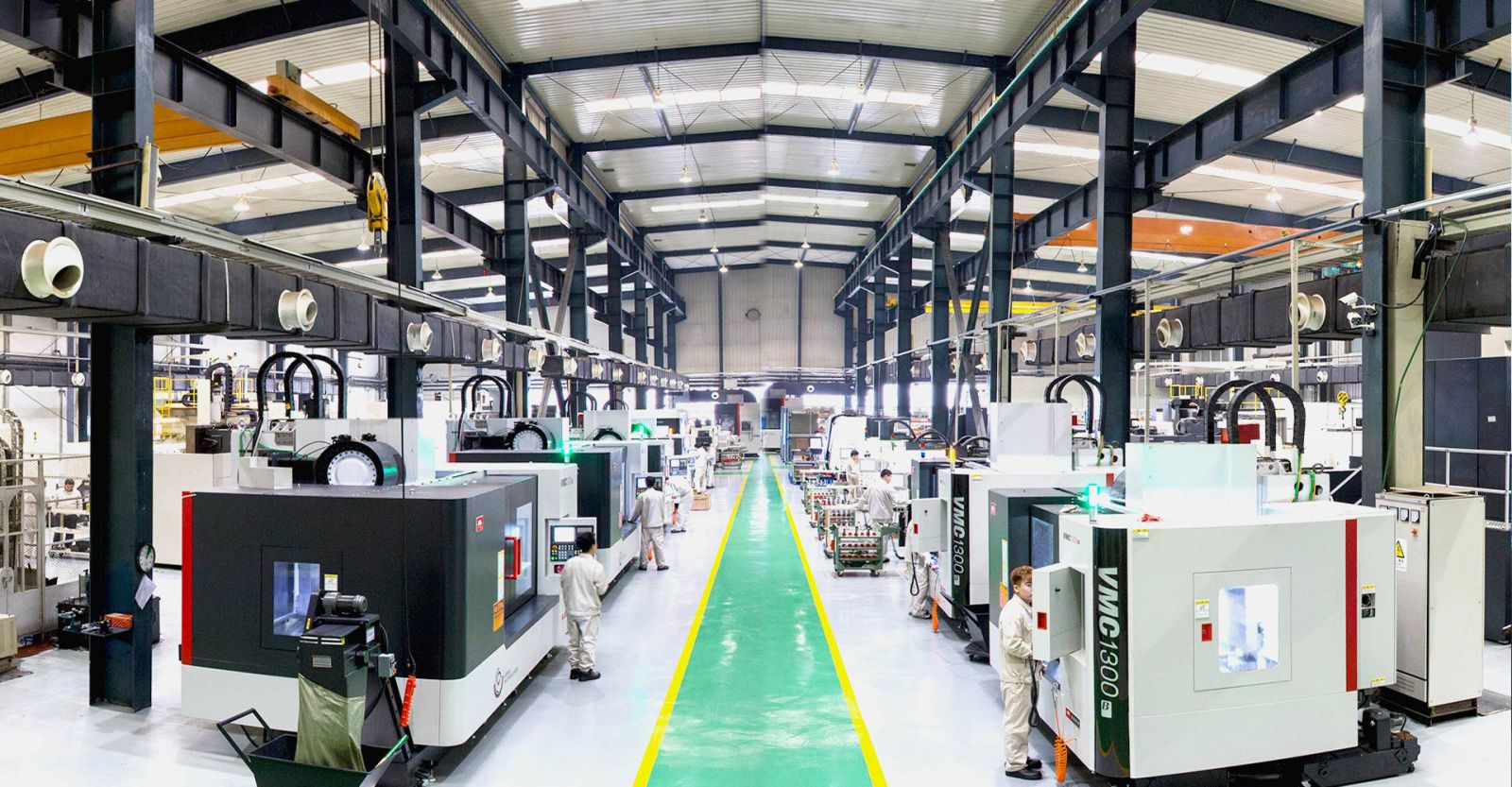
The geometry of semiconductor components frequently defies three-axis machining. Gas distribution manifolds incorporate intersecting internal passages at compound angles. Wafer handling end-effectors feature thin, sculpted profiles designed to minimize particle generation and wafer contact area. Vacuum chamber lids combine large planar sealing surfaces with complex mounting boss patterns.
Five-axis simultaneous machining allows we produce these features in a single setup, eliminating the datum shifts and accumulated tolerance stack-up that plague multi-operation workflows. For turned components such as precision vacuum flange fittings and threaded sensor housings, high-precision CNC turning with live tooling enables cross-drilling and milling without re-fixturing.
3.2 Strict Quality Assurance and Metrology
A machining capability claim is only as credible as the measurement infrastructure behind it. Yichou’s quality system is built around:
-
CMM inspection in climate-controlled environments using coordinate measuring machines with volumetric accuracy verified against calibrated artifacts.
-
Optical measurement for features inaccessible to contact probes, including small holes, thin walls, and surface finish parameters on complex geometries.
-
Roughness testing with calibrated profilometers.
-
Material certification and traceability from mill certificates through finished part serialization.
For semiconductor precision machining tolerances, the inspection plan is as important as the machining plan. Critical dimensions are identified on the drawing, measured at the appropriate stage of processing, and documented in an inspection report that accompanies each shipment.
3.3 DFM Support: Reducing Cost Without Compromising Performance
Design for Manufacturability review is where a capable machining partner adds value beyond executing a drawing. Common opportunities in semiconductor component design include:
-
Tolerance relaxation on non-critical features. A ±0.01 mm tolerance on a cosmetic edge costs far more to verify and hold than a ±0.05 mm tolerance that still meets fit and function.
-
Feature consolidation. Combining a separate bracket and spacer into a single machined component reduces assembly steps and eliminates a potential contamination trap.
-
Tool accessibility. Deep pockets with small corner radii require long, slender tools that deflect under cutting force. A minor radius increase can dramatically improve surface finish and reduce cycle time.
-
Material substitution. In non-critical applications, a lower-cost alloy or polymer may meet performance requirements while reducing both material and machining cost.
Yichou’s engineering team reviews customer CAD files and provides DFM feedback before quoting, ensuring that the quoted price reflects an optimized design rather than a rushed interpretation of the original drawing.
Section 4: Typical Semiconductor Components and Applications
The following categories represent the core of Yichou’s semiconductor equipment parts manufacturing experience.
Gas Distribution Manifolds and Showerheads. These components deliver process gases uniformly across the wafer surface. Internal passage geometry, surface finish, and freedom from burrs and contamination directly affect film uniformity. Machined from 316L VAR or aluminum, with electropolished or anodized finishes as required.
Wafer Handling End-Effectors and Vacuum Chucks. End-effectors must be lightweight, stiff, and particle-free. Materials range from aluminum with hard anodizing to PEEK and ceramic. Vacuum chucks require flatness and surface finish that ensure uniform wafer clamping without introducing stress.
High-Vacuum Chambers and Sensor Housings. Chamber bodies, lids, and viewport housings demand excellent sealing surface finish and dimensional stability under thermal cycling. Helium leak testing is performed on request.
RF Shield Enclosures and Heat Sinks. RF components require precise pocket depths and wall thicknesses to maintain impedance characteristics. Heat sinks demand flatness across the transistor mounting interface—typically 5 microns or better—to ensure uniform thermal interface material compression.
Precision Alignment Brackets and Mounting Hardware. Optical and beamline components require kinematic mounting features machined to tolerances that ensure repeatable repositioning.
Section 5: Conclusion and Call to Action
Selecting a machining partner for semiconductor equipment components is not a commodity decision. The consequences of inadequate tolerances, uncontrolled cleanliness, or undocumented material traceability propagate through the supply chain: equipment downtime at a fab, yield loss on a wafer lot, delayed tool qualification.
The characteristics that distinguish a qualified supplier are consistent across the industry. Climate-controlled machining and metrology. Proven experience with semiconductor-specific materials, particularly VAR-grade stainless and high-performance polymers. Cleaning and packaging protocols that maintain cleanliness from final inspection through customer receipt. And an engineering team that engages in DFM rather than simply quoting a drawing.
we has built its semiconductor CNC machining practice around these requirements. Whether you are sourcing prototypes of a new gas manifold design, scaling production of wafer handling components, or seeking a second source for existing part numbers, we are prepared to review your requirements and provide a detailed, DFM-informed quotation.
Ready to discuss your project?
Upload your CAD files and 2D drawings for a complimentary DFM assessment and quotation from our engineering team. For critical applications, we can provide sample inspection reports and material certifications for review before you place your first order.
Get Quote
- Visit our website: https://www.nbyichou.com/
- Email us: [email protected]
- Call us/whatsapp: +86 13355741031
- Chat with us: Live chat support available on our website