Silicon wafers: the unsung heroes behind our modern technological advancements. From smartphones to solar panels, these seemingly inconspicuous discs play a vital role in powering our digital era. But have you ever wondered about the journey of these humble wafers, and how they came to be the backbone of our technological progress? Join us as we dive into the fascinating evolution of silicon wafers – the driving force behind the ever-growing world of electronics. Discover how these thin slices of silicon have transformed from raw materials to highly sophisticated microchips, fueling our insatiable thirst for faster, smaller, and more efficient devices. Spanning decades of innovation, we'll trace the intricate manufacturing process and explore the exponential growth in performance and functionality that silicon wafers have enabled. Step into the heart of the electronics industry as we unravel the untold story of silicon wafers. From their humble beginnings to the present-day marvels, prepare to be amazed by the unassuming powerhouses that propel our lives forward. Don't miss this opportunity to gain a deeper understanding of the essential role these little gems play in shaping the technological landscape of tomorrow.
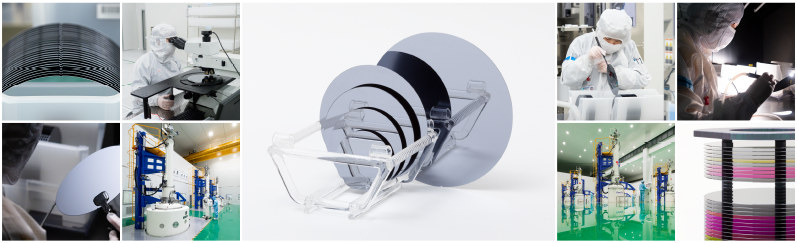
Title: The History of Silicon Wafers
Silicon wafers, the unsung heroes of modern technology, have a rich history dating back to the mid-20th century. The story of silicon wafers is intertwined with the rapid evolution of the electronics industry. These wafer-thin slices of crystalline silicon have played a pivotal role in shaping the digital age we live in today.
In the early days, silicon wafers were primarily used for semiconductors. Researchers and engineers at Bell Labs, such as William Shockley and John Bardeen, pioneered the development of the silicon transistor in the late 1940s. This groundbreaking invention marked the beginning of silicon's journey from obscurity to technological stardom.
As the demand for smaller, faster, and more efficient electronic devices grew, so did the need for improved silicon wafers. Over the years, the size of silicon wafers evolved, with the industry transitioning from small wafers measuring just a few inches in diameter to the standard 12-inch wafers used today. This evolution allowed manufacturers to produce more chips per wafer, significantly reducing costs and improving overall efficiency.
The history of silicon wafers is a testament to human innovation and the relentless pursuit of technological advancement. From their humble beginnings as simple semiconductors to their crucial role in powering everything from smartphones to supercomputers, silicon wafers have come a long way.
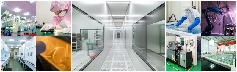
Title: The Structure and Manufacturing Process of Silicon Wafers
Silicon wafers may appear deceptively simple, but their structure and manufacturing process are anything but. To understand their significance, it's essential to delve into the intricate details of how these wafers are created.
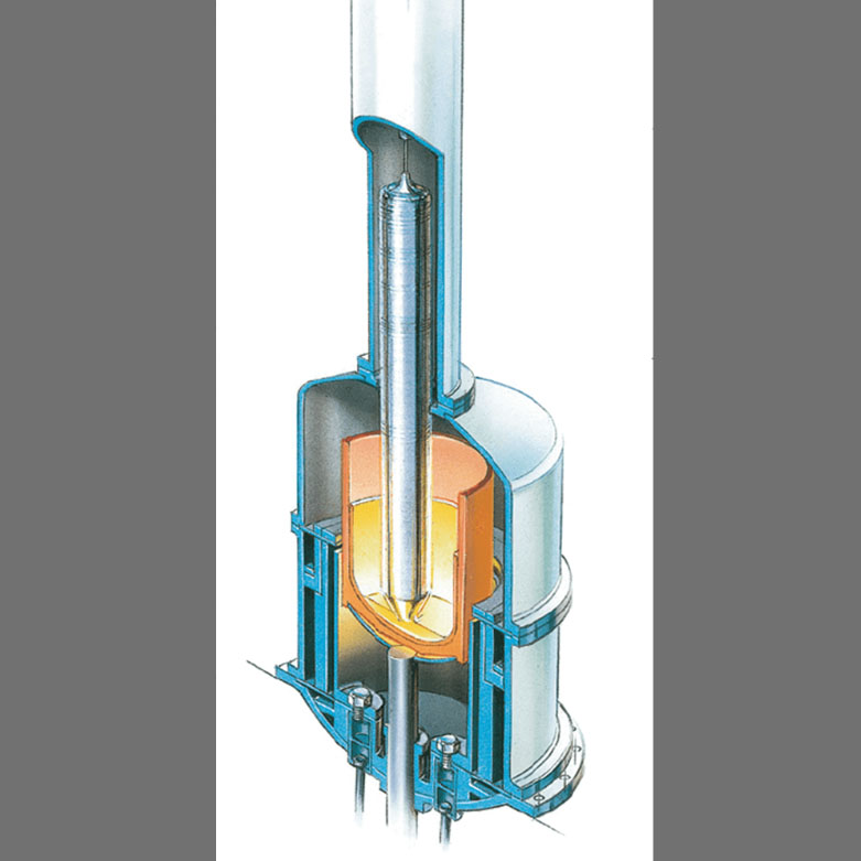
At its core, a silicon wafer is a thin, flat disc cut from a larger, cylindrical ingot of high-purity crystalline silicon. The quality of the silicon is paramount in determining the wafer's performance, with impurities being a significant concern. Manufacturing facilities meticulously purify the silicon to ensure it meets stringent industry standards.
The process of creating silicon wafers involves several critical steps. First, the silicon ingot is sliced into thin wafers using a precision saw. These wafers are then polished to achieve a smooth, mirror-like surface. This level of precision is essential to ensure the electronic components built on the wafer's surface function optimally.
One of the most crucial aspects of silicon wafer manufacturing is doping. Doping involves introducing specific elements, such as boron or phosphorus, into the silicon crystal lattice to alter its electrical properties. This process enables the creation of both p-type and n-type regions on the wafer, forming the basis of semiconductor devices like transistors.
Silicon wafers also undergo various cleaning and inspection stages to eliminate defects and imperfections. Advanced metrology tools are used to measure thickness, flatness, and other critical parameters to ensure the wafers meet the industry's stringent standards.
The intricacies of silicon wafer manufacturing underscore their importance as the foundation of modern electronics. A thorough understanding of the process is vital for optimizing the performance of electronic devices.
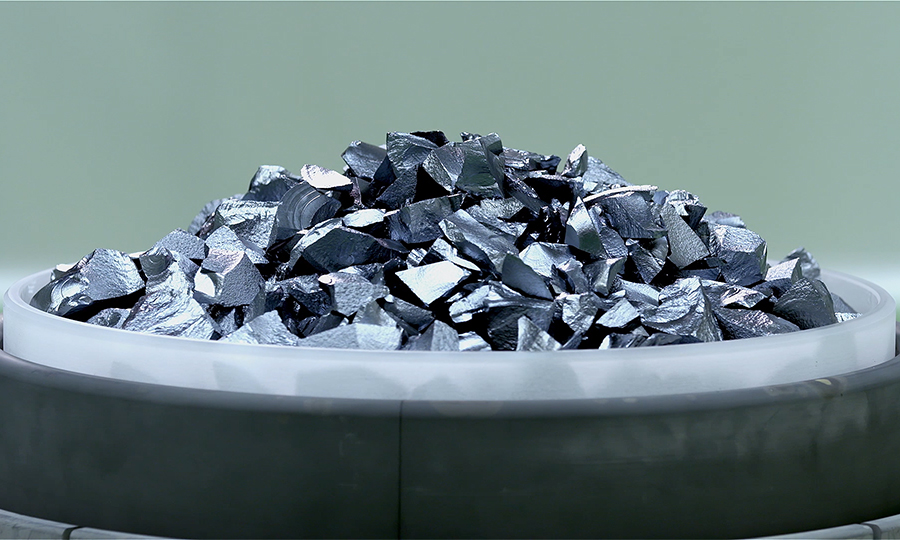
Title: The Importance of Silicon Wafers in Technology
In the realm of technology, silicon wafers are the unsung heroes that silently power the devices we rely on daily. Their importance cannot be overstated, as they serve as the backbone of virtually all electronic components, enabling the functionality of a wide array of devices, from smartphones to spacecraft.
Silicon wafers are the key building blocks of integrated circuits (ICs), which are the brains of electronic devices. These ICs contain transistors, capacitors, and resistors that control the flow of electrical signals. The miniaturization of these components, made possible by advancements in silicon wafer technology, has led to the creation of smaller and more powerful electronic devices.
One of the standout features of silicon wafers is their versatility. They can be customized to meet the specific needs of various applications, from high-performance computing to energy-efficient IoT devices. Silicon's exceptional electronic properties, combined with the precision of wafer manufacturing, make it the material of choice for electronic components.
Silicon wafers are also the linchpin of the semiconductor industry, a sector that drives technological innovation and economic growth. The rapid pace of advancements in semiconductor technology owes much to the continuous improvement of silicon wafer quality and manufacturing techniques.
In summary, silicon wafers are the foundation upon which the modern technological landscape is built. Their adaptability, reliability, and enduring presence make them an indispensable element of the digital age, shaping the world in ways we often take for granted.
Title: Applications of Silicon Wafers in Various Industries
Silicon wafers are not confined to a single industry; their versatility allows them to play a crucial role in diverse sectors, from telecommunications to healthcare. Let's explore the wide-ranging applications of silicon wafers and how they drive innovation across different fields.
-
Electronics: The most prominent application of silicon wafers is in the production of microchips and integrated circuits. These chips are at the heart of electronic devices such as smartphones, laptops, and gaming consoles. Silicon's excellent semiconductor properties, combined with the precise manufacturing of wafers, enable the creation of faster and more energy-efficient electronics.
-
Solar Energy: Silicon wafers are the primary material used in photovoltaic cells for solar panels. The ability of silicon to convert sunlight into electricity has revolutionized the renewable energy sector. Advances in wafer technology have led to higher solar panel efficiency and a more sustainable energy future.
-
Medical Devices: Silicon wafers find applications in medical devices such as sensors, imaging equipment, and lab-on-a-chip devices. Their biocompatibility and precision make them invaluable in the healthcare industry for diagnostic and therapeutic purposes.
-
Aerospace: Silicon wafers are used in aerospace technology for various applications, including sensors, communication systems, and navigation equipment. Their reliability and resistance to extreme conditions make them ideal for use in space exploration.
-
Automotive: Silicon wafers contribute to the advancement of automotive technology, powering components like engine control units (ECUs), sensors for autonomous driving, and entertainment systems. As the automotive industry transitions towards electric and autonomous vehicles, the demand for advanced silicon wafers continues to grow.
-
Telecommunications: Telecommunication networks rely on silicon wafers for signal processing, data transmission, and amplification. These wafers enable the rapid expansion and improvement of global communication networks.
-
Manufacturing: In the manufacturing sector, silicon wafers are used in precision equipment for metrology and quality control. Their role in ensuring high-quality production processes cannot be overstated.
The versatility of silicon wafers extends beyond these examples, touching nearly every aspect of modern life. As technology continues to evolve, so too will the applications of silicon wafers, driving innovation and progress in countless industries.
Title: Advancements in Silicon Wafer Technology
The evolution of silicon wafer technology has been nothing short of remarkable. Continuous advancements have propelled the industry forward, enabling smaller, more powerful, and energy-efficient electronic devices. Let's explore some of the key breakthroughs that have shaped the world of silicon wafers.
-
Shrinking Feature Sizes: One of the most significant advancements has been the continual reduction in feature sizes on silicon wafers. Moore's Law, proposed by Gordon Moore in 1965, predicted that the number of transistors on a silicon chip would double approximately every two years. This prediction has largely held true, driving innovation in the semiconductor industry.
-
FinFET Transistors: To overcome the limitations of traditional planar transistors, the industry introduced FinFET (fin field-effect transistor) technology. FinFETs have three-dimensional fin structures that improve control over the flow of electrical current, resulting in higher performance and energy efficiency.
-
Extreme Ultraviolet Lithography (EUV): EUV lithography is a cutting-edge technology that uses extremely short wavelengths of light to create finer patterns on silicon wafers. This technology has enabled the production of smaller and more densely packed transistors, pushing the boundaries of semiconductor miniaturization.
-
Advanced Materials: Silicon wafers have evolved from traditional crystalline silicon to include advanced materials like silicon-on-insulator (SOI) and gallium arsenide (GaAs). These materials offer unique properties that enhance the performance of semiconductor devices in specific applications.
-
3D Stacking: Three-dimensional stacking, or 3D ICs, involve layering multiple silicon wafers on top of each other. This vertical integration allows for more efficient use of space and improved interconnectivity, further boosting performance.
-
Advanced Packaging: The development of advanced packaging techniques, such as fan-out wafer-level packaging (FOWLP) and system-in-package (SiP), has enabled the integration of diverse components on a single silicon substrate, enhancing device functionality and reducing form factors.
These advancements have not only made electronic devices faster and more efficient but have also opened doors to entirely new technologies and applications. Silicon wafer technology remains at the forefront of innovation, driving progress in the digital age.
Title: Challenges and Future Trends in Silicon Wafer Production
While silicon wafer technology has seen remarkable progress, it is not without its challenges. Understanding these challenges and anticipating future trends is crucial for the continued success and sustainability of the industry. Let's delve into some of the key issues and emerging trends.
-
Increasing Complexity: As feature sizes on silicon wafers continue to shrink, the manufacturing process becomes increasingly complex and costly. Overcoming these challenges requires significant investments in research and development.
-
Economic and Environmental Concerns: The production of silicon wafers consumes substantial energy and resources, leading to environmental concerns. Manufacturers are under pressure to adopt more sustainable practices and reduce their carbon footprint.
-
Supply Chain Vulnerabilities: The semiconductor industry is highly interconnected, making it vulnerable to supply chain disruptions. Recent events, such as the global chip shortage, highlight the need for diversification and resilience in the supply chain.
-
Emerging Materials: As the demand for higher performance and energy efficiency grows, the industry is exploring new materials beyond traditional silicon. Innovations in materials like gallium nitride (GaN) and silicon carbide (SiC) are poised to shape the future of semiconductor technology.
-
Quantum Computing: Quantum computing represents a paradigm shift in computing power. While it's in its infancy, it has the potential to disrupt traditional silicon-based computing. The industry must monitor and adapt to this evolving landscape.
-
AI and Machine Learning: The integration of artificial intelligence (AI) and machine learning into various applications is driving demand for specialized silicon wafers designed for AI hardware accelerators. Meeting these requirements presents both challenges and opportunities.
-
Global Collaboration: Given the global nature of the semiconductor industry, collaboration between countries, companies, and research institutions will be crucial to addressing challenges and advancing technology.
The future of silicon wafer production lies in navigating these challenges while capitalizing on emerging trends. Sustainability, innovation, and adaptability will be key drivers in shaping the industry's trajectory.

Title: Environmental Impact of Silicon Wafer Manufacturing
The rapid expansion of the electronics industry, driven by the ubiquity of silicon-based devices, has raised concerns about the environmental impact of silicon wafer manufacturing. Understanding these impacts is vital for mitigating environmental harm and ensuring a sustainable future.
-
Energy Consumption: Silicon wafer manufacturing is energy-intensive, requiring significant electricity and heat. The production process involves melting, crystallizing, and cutting silicon, all of which demand substantial energy inputs. Transitioning to renewable energy sources and improving energy efficiency are essential steps to reduce this impact.
-
Water Usage: The semiconductor industry relies on vast quantities of ultra-pure water for various processes. Efficient water recycling and purification technologies are critical to minimize water consumption and mitigate the strain on local water resources.
-
Chemical Usage: Chemicals used in wafer manufacturing, including etchants, solvents, and dopants, can pose environmental risks if not handled properly. Stringent waste disposal and treatment protocols are essential to prevent pollution.
-
Waste Generation: The production process generates waste materials, including silicon dust and spent chemicals. Developing recycling and waste management programs can help minimize the environmental footprint.
-
Emission of Greenhouse Gases: Silicon wafer manufacturing facilities emit greenhouse gases, contributing to climate change. Implementing carbon capture and utilization (CCU) technologies can help offset these emissions.
-
Resource Depletion: The extraction of raw materials for silicon wafer production, such as silicon and quartz, can lead to resource depletion and habitat disruption. Sustainable sourcing practices and responsible mining are vital to address these issues.
-
Lifecycle Assessment: Conducting a comprehensive lifecycle assessment of silicon wafer manufacturing, from raw material extraction to end-of-life disposal, is crucial to identify and address environmental hotspots.
Addressing these environmental challenges requires a concerted effort from industry stakeholders, policymakers, and researchers. Sustainable practices, cleaner technologies, and circular economy principles will play pivotal roles in reducing the environmental impact of silicon wafer manufacturing.
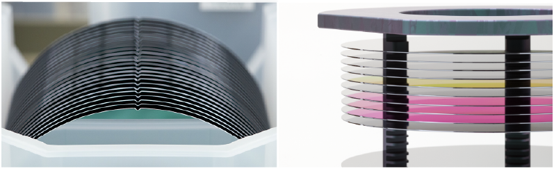
Title: Innovations and Alternatives to Silicon Wafers
In the ever-evolving landscape of technology, innovation is the driving force. Silicon wafers, while incredibly versatile, are not immune to competition from emerging materials and technologies. Let's explore some of the innovations and alternatives that are challenging the dominance of traditional silicon wafers.
-
Gallium Nitride (GaN): GaN is a wide-bandgap semiconductor material with properties that make it suitable for high-power and high-frequency applications. It is increasingly used in power electronics, LED lighting, and radio frequency (RF) devices. GaN's superior performance in certain areas poses a potential alternative to silicon wafers.
-
Silicon Carbide (SiC): SiC is another wide-bandgap semiconductor material known for its high-temperature tolerance and robustness. It is commonly used in power electronics and electric vehicle components. SiC wafers offer advantages in terms of efficiency and durability.
-
2D Materials: Materials like graphene and transition metal dichalcogenides (TMDs) are gaining attention for their unique electronic properties. While not yet practical for large-scale production, these materials hold promise for future electronic devices.
-
Quantum Dots: Quantum dots are nanoscale semiconductor particles with tunable properties. They are used in displays, lighting, and photovoltaics to enhance color accuracy and efficiency.
-
Carbon Nanotubes: Carbon nanotubes are cylindrical structures of carbon atoms known for their exceptional electrical and thermal properties. They have potential applications in transistors and interconnects.
-
Organic Electronics: Organic materials, such as organic semiconductors and polymers, are being explored for flexible and wearable electronics. These materials offer lightweight, bendable, and low-cost alternatives to traditional silicon.
-
Quantum Computing: Quantum computing, while in its infancy, has the potential to revolutionize computing. Quantum bits (qubits) offer unique advantages over classical bits, although practical implementation is still a challenge.
While these alternatives and innovations present exciting opportunities, silicon wafers remain the dominant technology due to their maturity, reliability, and extensive infrastructure. The coexistence of multiple materials and technologies will likely shape the future of electronics.
Conclusion: The Future of Silicon Wafers in Technology
In conclusion, silicon wafers have played an indispensable role in the evolution of modern technology. From their humble beginnings as semiconductors to their current status as the foundation of electronic devices, their journey is a testament to human innovation and perseverance.
The structure and manufacturing process of silicon wafers continue to evolve, enabling smaller, faster, and more energy-efficient electronic components. These advancements have driven progress in industries ranging from electronics and solar energy to healthcare and aerospace.
However, the industry faces significant challenges, including environmental concerns, supply chain vulnerabilities, and the emergence of alternative materials. Navigating these challenges while staying at the forefront of innovation will be crucial for the continued success of silicon wafer technology.
As we look to the future, it's clear that silicon wafers will remain a vital component of the technological landscape. Their adaptability, reliability, and versatility ensure their enduring relevance in a world driven by innovation and digital transformation. The story of silicon wafers is far from over, and their role in shaping the future of technology is bound to be as significant as their storied past.
FAQ 1: What Sets YICHOU Apart in the Silicon Wafer Industry?
At YICHOU, we distinguish ourselves through a profound historical legacy that spans decades, rooted in the heart of the silicon wafer industry. Our journey began with a vision of pushing the boundaries of technology, and today, it has evolved into a relentless pursuit of excellence. We've carved our niche as trailblazers in silicon wafer manufacturing, where every facet of our operation reflects our unwavering commitment to quality, innovation, and reliability.
Our journey has seen us weather the tides of change in silicon wafer technology, adapting and thriving amidst the industry's dynamic evolution. From the pioneering days of silicon transistors to the intricate world of nanotechnology, YICHOU has consistently demonstrated the agility to navigate these transformative shifts. Our resilience and adaptability have propelled us forward, making us a dependable pillar of the industry.
What truly sets us apart is our holistic approach to silicon wafers. We've embraced sustainability as a guiding principle, aligning our operations with eco-conscious practices. Our manufacturing processes are designed to optimize resource utilization and minimize environmental impact. This commitment to sustainable manufacturing reflects our awareness of the industry's responsibility in shaping a greener future.
Furthermore, YICHOU's dedication to innovation is unparalleled. Our research and development efforts continuously explore novel materials, manufacturing techniques, and cutting-edge technologies. This spirit of innovation ensures that we remain at the forefront of the industry, consistently delivering products that meet and exceed the ever-evolving demands of our diverse clientele.
In a world driven by technology, YICHOU's legacy, adaptability, commitment to sustainability, and relentless pursuit of innovation stand as pillars of strength, setting us apart in the silicon wafer industry.
FAQ 2: What Are the Key Advantages of YICHOU Silicon Wafers in Terms of Quality and Performance?
YICHOU silicon wafers epitomize the pinnacle of quality and performance in the semiconductor realm. Our unwavering dedication to excellence is reflected in every facet of our product, setting new standards in the industry.
When it comes to quality, our silicon wafers are forged from the purest silicon ingots, subjected to rigorous purification processes. This commitment to purity ensures that impurities do not compromise the integrity of our wafers, guaranteeing consistent and reliable performance.
Our precision cutting techniques are the hallmark of our manufacturing process. YICHOU wafers are renowned for their exceptional flatness and thickness uniformity. This level of precision allows for the production of integrated circuits with unparalleled reliability and efficiency. Whether it's for high-performance computing or cutting-edge telecommunications, our wafers consistently deliver excellence.
Performance is the beating heart of YICHOU silicon wafers. Our advanced doping techniques enable us to fine-tune the electrical properties of our wafers, catering to the specific needs of diverse applications. The result is wafers that empower semiconductor devices to operate at the peak of their capabilities.
Furthermore, we understand that performance goes beyond specifications; it extends to reliability over time. YICHOU wafers are engineered to withstand the rigors of real-world applications, ensuring longevity and consistent performance throughout the lifecycle of the devices they power.
In essence, YICHOU silicon wafers are more than just components; they are the embodiment of quality and performance that fuel technological advancements across industries.
FAQ 3: How Does YICHOU Address Environmental Concerns in Silicon Wafer Manufacturing?
At YICHOU, our commitment to environmental stewardship is deeply ingrained in our corporate DNA. We recognize the pivotal role the semiconductor industry plays in the global environmental landscape, and we are dedicated to minimizing our ecological footprint at every turn.
Energy conservation is a cornerstone of our sustainable manufacturing practices. Our production facilities are equipped with state-of-the-art energy-efficient technologies, and we continuously seek ways to optimize energy consumption. We are actively transitioning to renewable energy sources, further reducing our carbon emissions and reliance on fossil fuels.
Water, a precious resource, is managed with utmost care. YICHOU employs advanced water recycling and purification systems that minimize consumption and prevent contamination. We view water stewardship as a shared responsibility towards the preservation of this invaluable resource.
Our commitment to responsible chemical usage extends to every aspect of our operations. We have stringent protocols in place to ensure that chemicals are handled, stored, and disposed of with the utmost care and consideration for the environment. Waste management practices adhere to the highest standards to prevent pollution and minimize the impact on surrounding ecosystems.
Beyond our immediate operational practices, we actively invest in research and development focused on cleaner technologies and eco-friendly materials. Our goal is to pioneer the next generation of sustainable semiconductor manufacturing, setting new industry benchmarks for environmental responsibility.
YICHOU's dedication to environmental concerns is not just a commitment; it's a promise to contribute positively to the planet while continuing to deliver exceptional silicon wafers to our customers.
FAQ 4: What Are YICHOU's Plans for Embracing Emerging Technologies in Silicon Wafer Production?
YICHOU's journey in silicon wafer production is marked by an unwavering commitment to innovation. We recognize that staying at the forefront of technology requires proactive exploration and adaptation to emerging materials and manufacturing processes.
Alternative materials like gallium nitride (GaN) and silicon carbide (SiC) have garnered significant attention in recent years due to their unique properties. YICHOU is actively engaged in research and development efforts to harness the potential of these materials. Our goal is to provide our customers with a diverse range of options that align with the latest industry trends. These materials are poised to revolutionize various applications, from power electronics to renewable energy systems.
The world of 2D materials and quantum dots holds immense promise in the realm of semiconductor technology. YICHOU's research initiatives delve into these frontiers, exploring their potential in enhancing the performance of electronic devices. While these materials are not yet practical for large-scale production, our commitment to innovation means that we are actively shaping the future of silicon wafer technology.
Furthermore, YICHOU recognizes that embracing emerging technologies goes beyond materials. We are investing in advanced manufacturing processes, automation, and artificial intelligence to enhance the efficiency and precision of our production. These advancements not only improve our manufacturing capabilities but also contribute to the overall progress of the semiconductor industry.
In essence, YICHOU's plans for embracing emerging technologies are a testament to our proactive approach to innovation. We are not just keeping pace with change; we are driving it, ensuring that our customers have access to the most advanced solutions in silicon wafer production.
FAQ 5: How Does YICHOU Ensure a Reliable Supply Chain in the Semiconductor Industry?
In the semiconductor industry, the reliability of the supply chain is paramount, and YICHOU understands this at its core. Our commitment to ensuring a dependable supply chain is multifaceted and comprehensive.
Diversification is a key strategy in mitigating supply chain risks. YICHOU strategically sources materials from multiple suppliers and maintains multiple production facilities across geographically diverse locations. This approach enhances our resilience against disruptions, ensuring a continuous flow of essential materials and components.
Collaboration is a cornerstone of our supply chain management. We have cultivated strong partnerships with leading institutions and companies in the semiconductor ecosystem. These collaborations provide us with valuable insights, early access to emerging technologies, and a network of support that bolsters our supply chain stability.
Our approach to supply chain management is proactive, focusing on risk assessment and mitigation. We continuously monitor global trends and potential disruptions, allowing us to adapt swiftly to changing circumstances. By identifying vulnerabilities and implementing robust contingency plans, YICHOU is prepared to navigate even the most challenging supply chain scenarios.
Customer-centricity is ingrained in our supply chain philosophy. We prioritize open communication with our customers, ensuring transparency and responsiveness. By understanding their needs and requirements, we can tailor our supply chain strategies to meet specific demands and deliver on our commitments.
In conclusion, YICHOU's approach to ensuring a reliable supply chain is a testament to our dedication to our customers' success. We understand that our role extends beyond being a supplier; we are a trusted partner, committed to delivering consistent, high-quality silicon wafers, regardless of the challenges that may arise in the dynamic semiconductor landscape.