Ultra-High Vacuum Chamber CNC Machining: Surface Roughness, Material Selection, and Manufacturing Excellence for Semiconductor Equipment
The semiconductor industry is experiencing an unprecedented surge in demand for advanced chip manufacturing capabilities. Artificial intelligence accelerators, 5G infrastructure, autonomous vehicle processors, and high-performance computing systems all require cutting-edge silicon fabricated at nodes below 5 nanometers. At these microscopic scales, the manufacturing environment must achieve near-perfect purity and stability. This is why ultra-high vacuum technology has become the backbone of modern semiconductor fabrication.
For procurement managers, supply chain engineers, and R&D specialists at global chip equipment OEMs, understanding the nuances of CNC machined UHV chamber manufacturing is no longer optional—it is essential for ensuring yield rates, reducing downtime, and maintaining competitive advantage.
This comprehensive guide examines every critical aspect of UHV chamber production, from material selection and rough machining to surface finishing, metrology, and cleanroom assembly. We explore why surface roughness is arguably the most important quality metric in this domain and how world-class CNC machining for semiconductor equipment suppliers consistently achieve sub-micron precision.
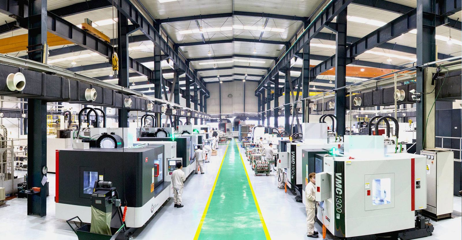
.jpeg)
Part 1: Understanding Ultra-High Vacuum and Its Demanding Requirements
What Defines an Ultra-High Vacuum Environment?
Ultra-high vacuum is defined as pressures below 10⁻⁷ Pa (roughly 10⁻⁹ mbar or 10⁻¹² Torr). At these extreme pressure levels, the mean free path of gas molecules exceeds several kilometers, meaning molecular collisions become negligible. This creates an environment where semiconductor deposition, etching, and lithography processes can proceed without contamination from ambient gases.
To put this in perspective, a UHV chamber at 10⁻⁹ Pa contains fewer than 10⁵ molecules per cubic centimeter—a near-perfect void compared to atmospheric conditions, which contain approximately 10¹⁹ molecules per cubic centimeter. Achieving and maintaining such a pristine environment requires hardware of extraordinary quality.
Why Traditional Machining Fails for UHV Applications
The gap between standard industrial machining and UHV-grade precision manufacturing is vast. Traditional CNC machine shops focus primarily on geometric accuracy—ensuring holes are in the right place and surfaces are flat to within a few hundredths of a millimeter. For UHV chambers, this approach is entirely inadequate.
Consider the physics of outgassing. Every surface has microscopic peaks and valleys. When a rough surface is exposed to air, gas molecules become trapped in these microscopic cavities. When the chamber is evacuated, these trapped molecules slowly release—a process that can continue for weeks or months. This phenomenon, known as outgassing, is the single greatest obstacle to achieving stable UHV pressures.
The relationship is straightforward: rougher surfaces = higher outgassing rates = longer pump-down times = lower throughput and higher operating costs.
For semiconductor fabs operating 24/7/365, pump-down time directly translates into lost revenue. A chamber that requires an extra four hours to reach operational vacuum can reduce annual throughput by hundreds of wafer starts. This is why the industry standard for UHV chamber surface finish has steadily tightened from Ra 0.4 μm to Ra 0.1 μm and, in critical applications, Ra 0.025 μm.
Part 2: Material Selection for UHV Chamber Manufacturing
Aluminum Alloys: 6061-T6 and Beyond
6061-T6 aluminum is the predominant choice for large UHV chambers, particularly in semiconductor manufacturing where weight reduction is valuable. This precipitation-hardened alloy offers several properties essential for vacuum service:
-
Low hydrogen permeability: Hydrogen is the most problematic residual gas in UHV systems, and 6061-T6 exhibits lower hydrogen diffusion rates than many other aluminum alloys.
-
Excellent machinability: The alloy produces clean chips and allows for high cutting speeds, essential for the aggressive material removal required in chamber fabrication.
-
Thermal stability: When properly heat-treated and stress-relieved, 6061-T6 maintains dimensional stability across the temperature excursions common in semiconductor processing.
-
Compatibility with anodization: A hard-anodized surface can improve wear resistance and reduce outgassing.
However, aluminum poses significant machining challenges. The material's relatively high coefficient of thermal expansion (23.6 μm/m·°C) means that temperature control during machining is absolutely critical. A temperature variation of just 2°C across a 1-meter chamber can produce 47 μm of thermal growth—enough to compromise critical internal features.
Stainless Steel Alloys: 316L and 316LN
For applications requiring higher structural strength, corrosion resistance, or compatibility with particularly aggressive process gases, 316L and 316LN stainless steel are the standards. These low-carbon austenitic steels offer:
-
Superior hydrogen resistance: Lower hydrogen permeability compared to aluminum
-
Higher temperature capability: Suitable for processes requiring elevated temperatures
-
Exceptional corrosion resistance: Particularly important in etching and cleaning applications
-
Lower thermal expansion: Approximately 16 μm/m·°C, roughly 30% lower than aluminum
The key machining considerations for stainless steel UHV components are significantly different from aluminum. Stainless steel work-hardens rapidly, meaning that improper feed rates or tool geometry can lead to work-hardened surface layers that subsequently cause tool failure and dimensional inaccuracies. This is why dedicated precision CNC machining with micron-level tolerances for semiconductor tools demands specific toolpath strategies for each material.
Material Certification and Traceability
For semiconductor equipment, material certification is non-negotiable. Every incoming block of aluminum or stainless steel must be accompanied by mill test reports verifying:
-
Chemical composition to ensure the material meets the specified alloy requirements
-
Mechanical properties including yield strength, tensile strength, and elongation
-
Grain structure and inclusion rating to ensure material homogeneity
-
Hydrogen content to guarantee low outgassing potential
Many leading OEMs now require that the material be sourced from specific mills with approved quality management systems. The ability to provide full material traceability—from the mill to the final machined component—is a baseline qualification for any UHV chamber supplier serving the semiconductor industry.
Part 3: The UHV Chamber Manufacturing Process—A Step-by-Step Overview
Phase 1: Raw Material Preparation
The manufacturing process begins with the selection and preparation of raw forging or plate stock. For large chambers (diameters exceeding 800 mm), forged rings provide superior grain structure compared to plate material. For smaller chambers, rolled plate is often acceptable.
Initial inspection includes ultrasonic testing to detect internal voids, inclusions, or delaminations. Even a single inclusion can become a leak path or a particle source in the finished chamber, so this inspection is mandatory for UHV applications.
Phase 2: Roughing Operations
The roughing phase is where the vast majority of material is removed. For a monolithically machined chamber, the starting block may weigh 2,000 kg; the finished chamber, when complete, may weigh only 400 kg. This material removal—amounting to 80% of the original stock—must be performed with careful consideration of residual stress management.
Key roughing considerations:
-
Tool selection: Large-diameter indexable milling cutters with specialized carbide inserts remove material at high metal removal rates (MRR exceeding 500 cm³/min in aluminum).
-
Cutting parameters: High feed rates with moderate depths of cut minimize heat generation and thermal stress in the workpiece.
-
Stress relief intervals: Progressive roughing with intermediate stress-relief heat treatments allows residual stresses to equalize before critical finishing operations.
Phase 3: Stress Relief and Stabilization
This intermediate phase is where many manufacturers fall short. After the majority of material has been removed, the part's internal stress distribution has been significantly altered. Without proper stabilization, the final dimensions will shift over time.
The standard approach involves:
-
Thermal stress relief: Heating the workpiece to temperatures below its precipitation-hardening temperature (for aluminum) or below sensitization temperature (for stainless steel)
-
Cryogenic stabilization: Alternating between elevated and sub-zero temperatures to accelerate stress relaxation
-
Vibration stress relief: Applying mechanical vibration to relax internal stresses (a technique particularly effective for large weldments)
Each technique has its advantages, and leading manufacturers employ a combination based on the specific material and geometry of the chamber.
Phase 4: Semi-Finishing
Following stress relief, the chamber returns to the machine for semi-finishing operations. At this stage, all critical datums are established, and most internal features are roughed in. The goal is to approach the final dimensions while leaving approximately 0.5 mm of stock for the final finishing pass.
This stage requires 5-axis CNC machining for ultra-high vacuum equipment to access complex internal geometries. A 5-axis machine allows the cutter to remain perpendicular to the surface at all times, eliminating the scallop marks that would result from 3-axis machining and improving subsequent surface finishing capabilities.
Phase 5: Final Finishing
The finishing phase is where surface quality is defined. Using specialized tool geometries, optimized cutting parameters, and tight coolant control, the machine removes the final 0.5 mm of stock to achieve the specified surface finish and dimensional tolerances.
Critical finishing parameters:
| Parameter | Typical Range | Impact on Result |
|---|---|---|
| Cutting speed (aluminum) | 1,000-2,500 m/min | Higher speeds produce better surface finish |
| Cutting speed (stainless) | 200-400 m/min | Lower speeds manage work-hardening |
| Feed per tooth | 0.02-0.08 mm/tooth | Lower feed improves surface finish |
| Depth of cut | 0.05-0.25 mm | Shallow cuts reduce tool deflection |
| Coolant pressure | 50-100 bar | High pressure ensures chip evacuation |
The selection of polycrystalline diamond (PCD) tooling for aluminum finishing provides the wear resistance and edge sharpness necessary for consistent surface quality. PCD tooling maintains its cutting edge for thousands of passes, unlike carbide tools which progressively wear and degrade surface finish.
Phase 6: Weld Preparation and Assembly (If Applicable)
While monolithic chambers are preferred for their absence of joints, practical constraints often require welding. Large chambers may be machined in sections and welded together, or internal components may be attached via electron beam or TIG welding.
For UHV welding, the process must be:
-
Full penetration: No trapped volumes where gas could accumulate
-
Weld-repaired only: Defects cannot be filled—they must be removed and re-welded
-
Inert atmosphere shielded: No oxidation or contamination of the weld zone
-
Distortion controlled: The welding heat input must not compromise chamber geometry
Part 4: Surface Finish and Ra Value—The Critical Metric
Understanding Surface Roughness Parameters
While Ra (average roughness) is the most commonly specified parameter, it is not the only one that matters. UHV components are increasingly specified with additional parameters:
-
Rz (average maximum height): Provides information about the deepest valleys on the surface
-
Rp (maximum peak height): Critical for contact seals and sliding surfaces
-
Rq (root mean square roughness): More sensitive to occasional high peaks than Ra
-
Rsk (skewness): Indicates whether the surface has more peaks or valleys
For UHV applications, an ideal surface has negative skew—meaning it consists primarily of valleys with no high peaks. These valleys provide bearing area while minimizing the sharp peaks that can shed particles.
Surface Finish vs. Outgassing Rate—The Quantitative Relationship
The relationship between surface roughness and outgassing rate is well-established in vacuum science. For machined metallic surfaces, outgassing rate is approximately proportional to the surface area—and the effective surface area increases with roughness.
The "real" surface area of a rough surface can be 3-10 times greater than its projected area. This multiplier translates directly into increased outgassing.
Comparative outgassing rates by surface finish:
| Surface Finish | Approximate Effective Area Ratio | Typical Outgassing Rate (Pa·m³/s·m²) |
|---|---|---|
| As-machined (Ra 3.2 μm) | 5-10x | 5 × 10⁻⁸ |
| Precision machined (Ra 0.8 μm) | 2-3x | 1 × 10⁻⁸ |
| Fine machined (Ra 0.2 μm) | 1.3-1.5x | 5 × 10⁻⁹ |
| Superfinished (Ra 0.05 μm) | 1.1-1.2x | 2 × 10⁻⁹ |
These numbers demonstrate that reducing Ra from 3.2 μm to 0.05 μm can decrease outgassing by more than a factor of 20. This translates to dramatically faster pump-down, quicker process stabilization, and higher equipment utilization.
Achieving Ra ≤ 0.1 μm in Production
Repeatedly achieving Ra ≤ 0.1 μm across the full internal surface of a large UHV chamber is a significant manufacturing challenge. Here's how world-class shops accomplish this:
1. Machine Rigidity: The machine tool must be massive enough to resist deflection from cutting forces. A 5-axis machine weighing 20 tons or more is typical for large chamber work.
2. Spindle Speed and Power: Surface finish in milling improves with cutting speed. Spindles capable of 20,000 RPM or more (with high torque at those speeds) allow the use of small-diameter finishing tools.
3. Tool Path Optimization: Advanced CAM software calculates tool paths that maintain consistent tool engagement, reducing vibration marks and maintaining consistent finish across the entire surface.
4. Vibration Damping: Machine structure damping—including polymer concrete bases and active vibration isolation—prevents chatter that would ruin surface finish.
5. Process Monitoring: In-process monitoring of spindle load, tool wear, and vibration allows automatic adjustment of cutting parameters to maintain finish quality.
Electropolishing and Mechanical Finishing
For applications requiring even smoother surfaces than machining can reliably provide, electropolishing is the preferred solution. This electrochemical process removes a thin layer of material (typically 10-30 μm) from the surface, dissolving the microscopic peaks preferentially.
Benefits of electropolishing for UHV:
-
Eliminates the "directional" pattern left by machining
-
Removes embedded cutting fluid and contaminants
-
Passivates stainless steel surfaces, improving corrosion resistance
-
Achieves Ra values below 0.025 μm
The combination of precision machining followed by electropolishing is now the industry standard for critical UHV components in advanced semiconductor equipment.
Part 5: Advanced CNC Machining Capabilities for Semiconductor Components
Multi-Axis Machining of Complex Geometries
Modern semiconductor chambers are far from simple boxes. Internal cooling channels, complex gas distribution paths, and intricate mounting features all require advanced machine capabilities.
5-axis simultaneous machining enables the creation of features that would be impossible with 3-axis machines:
-
Undercuts and back faces: Features behind other features can be machined without secondary setups
-
Compound angles: Gas injection ports and feedthroughs at multiple angles
-
Thin-walled structures: Complex internal geometries with optimized wall thickness for thermal management
-
Direct machining of curved sealing surfaces: Eliminating the need for separate seal rings
The ability to produce these complex features in a single setup dramatically improves accuracy. Each setup change introduces opportunities for misalignment and cumulative error.
Micro-Machining of Wafer Handling Components
Precision CNC machined wafer chucks and Electrostatic chuck (ESC) base plates represent some of the most demanding machining tasks in the industry. These components may have:
-
Hundreds of precisely drilled gas holes (0.1-0.3 mm diameter)
-
0.5-1.0 μm flatness across 300 mm diameters
-
Surface finishes below Ra 0.05 μm
-
Complex cooling channel patterns for temperature control
Micro-machining of these components requires:
-
High-speed spindles capable of 60,000 RPM or more
-
Precision tool setting with tool touch-off accuracy better than 0.001 mm
-
Thermal management in both the machine and the workpiece
-
In-process measurement to verify dimensions at each step
Machining of High-Purity Gas Distribution Components
High-purity gas box components for semiconductor processing demand a different set of considerations. These components, which control the flow of process gases into the chamber, must have:
-
Surface finishes better than Ra 0.2 μm to prevent adsorption of reactive gases
-
Ultra-clean internal surfaces free of machining residues
-
Precision sealing surfaces for leak-free connections
-
Materials compatible with process gases (often aluminum or specialized alloys)
The machining of these components must be performed in controlled environments, often with filtered air systems to prevent contamination of the workpiece.
Part 6: Metrology and Quality Assurance
Dimensional Inspection
The dimensional tolerances on UHV components are extraordinarily tight. Most critical dimensions are specified with tolerances of ±0.01 mm, with some features approaching ±0.005 mm.
CMM verification of these components requires:
-
Climate-controlled metrology laboratories maintained at 20°C ± 0.5°C
-
High-accuracy scanning probes with certified calibration
-
Temperature-compensated measurements accounting for thermal expansion
-
Statistical process control to identify trends and prevent defects
For wafer chucks and ESC plates, flatness measurement is typically performed using laser interferometers. The measurement resolution must be better than 0.1 μm to verify flatness claims.
Surface Finish Measurement
Surface finish is typically measured using:
-
Contact profilometers for Ra, Rz, and Rq measurement
-
Atomic force microscopes for surfaces requiring sub-nanometer characterization
-
White-light interferometers for non-contact, high-resolution measurement
For UHV components, surface finish measurements are typically performed at multiple locations across the component surface. Statistical evaluation confirms that the entire surface meets the specification.
Leak Testing
Helium leak testing remains the gold standard for verifying vacuum integrity. The testing procedure includes:
-
Pressurization: The chamber is pressurized with helium
-
Sniffing: A mass spectrometer sniffer is moved across all potential leak paths
-
Quantification: Any detected leaks are quantified
-
Resolution: Leak locations are identified for potential repair
Acceptable leak rates for semiconductor UHV chambers typically range from 1×10⁻⁹ to 1×10⁻¹¹ Pa·m³/s, depending on the specific application.
Cleanliness Verification
The cleanliness of UHV components is verified through:
-
Residual gas analysis: Examining any gases released by the component
-
Particulate counting: Using particle counters in cleanroom environments
-
Organic contamination testing: Using FTIR or GCMS to detect hydrocarbon residues
-
Ion chromatography: Detecting ionic residues from cleaning processes
These tests ensure that the component will not introduce contaminants into the semiconductor processing environment.
Part 7: Cleanroom Assembly and Packaging
Cleanroom Classifications
The assembly of UHV components requires cleanroom conditions:
-
ISO Class 5 (Class 100) for final assembly and packaging
-
ISO Class 6 (Class 1,000) for intermediate assembly
-
ISO Class 7 (Class 10,000) for general handling
These classifications require HEPA or ULPA filtration, positive pressure, and strict gowning procedures for all personnel entering the area.
Assembly Procedures
During cleanroom assembly:
-
All components are cleaned in multi-stage processes (ultrasonic degreasing, deionized water rinsing, drying)
-
Assembly is performed using cleanroom-compatible tools and procedures
-
O-rings and seals are installed using powder-free, semiconductor-grade gloves
-
Threads are treated with vacuum-compatible lubricants (if used at all)
Packaging for Delivery
Final packaging for UHV components must preserve the cleanliness achieved during manufacturing:
-
Double vacuum bagging with heat-sealed polyethylene film
-
Desiccant packets to prevent moisture absorption during transport
-
Argon backfilling to provide an inert atmosphere
-
External packaging with foam or vibration-dampening material
The packaged components must arrive at the customer facility ready for immediate use—no cleaning, no preparation, no risk of contamination.
Part 8: Design for Manufacturing (DFM) Considerations
Why DFM Matters for UHV Components
Many UHV components are designed without full consideration of how they will be manufactured. This often leads to:
-
Unnecessarily complex toolpaths requiring extended machining time
-
Features that are difficult to inspect or measure
-
Critical surfaces that cannot be accessed by finishing tools
-
Stress concentrations that make the component more prone to distortion
Early collaboration with a precision CNC machining for semiconductor tools supplier can identify these issues before they become problems.
Critical DFM Guidelines for UHV Components
-
Avoid internal corners smaller than 3 mm radius unless absolutely necessary
-
Consider how the chamber will be held during machining (fixturing points)
-
Provide access for measurement tools to all critical surfaces
-
Specify realistic tolerances (tight tolerances on non-critical surfaces add cost without benefit)
-
Consider material suppliers with proven quality
The DFM Feedback Process
When a customer submits a STEP file or 2D drawing for Design for Manufacturing feedback, a knowledgeable supplier will evaluate:
-
Whether the tolerances are achievable with standard processes
-
Whether the design includes features that could be simplified
-
Whether the material selection is optimal for the application
-
Whether the surfaces requiring specific finishes are accessible
-
Whether the design provides adequate fixturing points
This feedback can reduce manufacturing time by 20-40% and significantly improve first-pass yield.
Part 9: Selecting a Tier-1 UHV Chamber Manufacturing Partner
Capabilities to Evaluate
When evaluating potential suppliers for UHV chamber manufacturing, consider:
-
Machine capacity: Does the supplier have machines large enough for your chambers? Do they have redundant capacity?
-
Experience: How many UHV chambers have they manufactured? What materials have they worked with?
-
Quality systems: Do they maintain ISO 9001, ISO 13485, or AS9100 certification? What about internal quality metrics?
-
Measurement capability: What measurement equipment do they have? Is it calibrated and traceable?
-
Cleanroom access: Do they have cleanroom assembly and packaging capabilities?
-
Supply chain: Can they obtain certified materials consistently?
Questions to Ask Potential Suppliers
-
What is your typical surface finish capability on 6061-T6? On 316L?
-
How do you manage residual stress in large chamber machining?
-
What is your standard delivery lead time for components of this size and complexity?
-
Can you provide references from semiconductor equipment manufacturers?
-
How do you handle changes or modifications during the manufacturing process?
-
What is your policy on NDA protection and IP confidentiality?
The Cost of Quality
For UHV components, the lowest price is rarely the best value. Consider:
-
Cost of failure: A defective chamber component can cause millions in downtime
-
Cost of schedule slip: Late delivery may delay equipment installation
-
Cost of poor quality: Components that fail inspection require rework or replacement
A reputable UHV chamber supplier should be able to justify its pricing through demonstrated quality, reliability, and technical expertise.
Part 10: The Future of UHV Chamber Manufacturing
Trends in the Semiconductor Industry
Several trends are shaping the future of UHV chamber manufacturing:
-
Larger chambers for processing 300 mm wafers and emerging larger substrates
-
More complex geometries to enable new deposition and etching capabilities
-
Tighter tolerances as feature sizes shrink further
-
New materials including refractory metals and advanced alloys
Advancing Manufacturing Technologies
The manufacturing processes themselves are evolving:
-
Additive manufacturing for producing near-net shape blanks that require less machining
-
Artificial intelligence for toolpath optimization and process control
-
Advanced automation for lights-out manufacturing and 24/7 production
-
Digital twins for predicting and controlling component behavior
Sustainability Considerations
Environmental considerations are increasingly important:
-
Material utilization (minimizing scrap through near-net shape processes)
-
Energy consumption in manufacturing facilities
-
Recycling of machining waste and packaging materials
-
Process optimization to minimize material waste
Conclusion: Engineering Excellence for Semiconductor Manufacturing
The manufacturing of CNC machined Ultra-High Vacuum chambers and components represents one of the most demanding metalworking challenges in modern industry. From raw material selection through final cleanroom packaging, every step must be executed with precision, consistency, and attention to detail.
Surface roughness, while often overlooked by casual observers, is perhaps the single most important quality metric for UHV components. Achieving Ra values below 0.1 μm—and often below 0.025 μm—requires not just advanced machines and tools, but deep technical expertise, rigorous process control, and an unwavering commitment to quality.
For procurement managers and engineers responsible for semiconductor equipment manufacturing, partnering with a qualified, experienced supplier is essential. The right partner brings not just manufacturing capability, but design expertise, quality assurance, and the reliability needed to keep your production lines moving.
Frequently Asked Questions
Q: What is the standard surface finish for UHV chambers in semiconductor applications?
A: While specific requirements vary, most semiconductor UHV chambers require internal surface finishes of Ra 0.2 μm or better. Critical components like wafer chucks or ESC plates typically require Ra 0.05 μm or better.
Q: Why can't standard CNC machine shops produce UHV components?
A: UHV components require specialized capabilities including temperature-controlled machining, multi-stage stress relief, precision metrology, and cleanroom assembly. Most standard shops lack these capabilities.
Q: How much does a custom CNC machined UHV chamber cost?
A: Pricing varies widely based on size, complexity, material, and quantity. Large chambers can exceed $100,000 each, while smaller components may cost from a few thousand dollars.
Q: What is the typical lead time for UHV chamber manufacturing?
A: For large, complex chambers, expect 8-16 weeks from design approval to delivery. Smaller components may be deliverable in 4-6 weeks.
Q: How do I ensure my component design is manufacturable?
A: Submit your design to a qualified supplier for Design for Manufacturing (DFM) feedback before finalizing the design. This can identify potential issues before they become costly problems.
Ready to Start Your UHV Component Project?
Our facility combines advanced 5-axis machining centers with decades of expertise in UHV chamber manufacturing. We serve semiconductor equipment OEMs globally, providing precision components with full traceability, certification, and cleanroom packaging.
Contact our engineering team today to discuss your project requirements. Submit your NDA-protected STEP or IGS file and receive professional DFM feedback and a comprehensive quote within 24 hours.
Get Quote
- Visit our website: https://www.nbyichou.com/
- Email us: [email protected]
- Call us/whatsapp: +86 13355741031
- Chat with us: Live chat support available on our website